


Recently, several colleagues have asked me the same question: How can we improve BGA design to strengthen solder joints and prevent BGA solder ball cracking?
The question came up after a senior executive made it clear during a product development meeting that someone would have to take responsibility if customers continued to report BGA cracking issues. This kind of reaction is not uncommon in product development, but it raises a more important question: Are we addressing the root cause, or are we simply putting more pressure on the engineering team?
Many companies want products to be thinner, lighter, and more compact while continuously shortening development schedules. A new product development cycle that once took 12 months may be compressed to nine months and then further reduced to six months through a shift-left approach. Meanwhile, industrial design (ID) requirements keep changing, schedules are not allowed to slip, and the finished product is still expected to be flawless.
Under these conditions, engineers are often left struggling to meet conflicting demands. Instead of expecting engineers to solve every problem through manufacturing adjustments alone, companies should address mechanical design, PCB layout, material selection, and product reliability early in development.
Workingbear has already published several articles on BGA detachment, soldering defects, and BGA solder ball cracking. However, I have not yet put together a comprehensive overview of design approaches for strengthening BGAs and preventing solder joint cracking. That is what this article aims to address.
Before discussing possible design improvements, we first need to understand why BGA solder joints crack. Let’s assume that manufacturing-related issues have been ruled out: all BGA solder joints were properly formed, and the intermetallic compound (IMC) formation is normal. If BGA cracking still occurs under these conditions, the primary factor to investigate is mechanical stress.
Workingbear reaches this conclusion based on the failure analyses I have conducted. In many cases, component detachment and solder joint cracking are closely related to mechanical stress, even when the soldering process itself appears to be acceptable.
Common Sources of Stress That Cause Component Detachment and Solder Joint Cracking
-
Residual stress from manufacturing and material deformation
For example, the PCB or BGA package may warp during high-temperature reflow. As the materials heat up and cool down, they deform differently because of their different coefficients of thermal expansion (CTE). The resulting stress may gradually relax until the structure reaches a new equilibrium. In some cases, however, a solder joint may crack before that equilibrium is reached. -
External impact or mechanical loading
Consider a smartphone. The PCB may bend when the phone is subjected to pressure in a user’s pocket, as illustrated by the well-known iPhone 6 Plus bending controversy. Accidental drops can also generate significant impact forces that damage BGA solder joints. -
Thermal stress caused by environmental temperature changes
In some regions, outdoor temperatures can fall below freezing during winter. Moving a product from a heated indoor environment to freezing outdoor conditions can cause a rapid temperature change. In tropical regions, a similar problem can occur when moving a product from an air-conditioned room into hot outdoor conditions. Products left inside a vehicle may experience even greater temperature swings as the interior heats up during the day and cools down at night.
Temperature changes matter because different materials have different coefficients of thermal expansion (CTE). The PCB laminate, solder balls, and BGA package materials do not expand or contract at the same rate. This mismatch generates stress in the solder joints.
Bridges and other structures use expansion joints to accommodate thermal expansion and contraction. Electronic assemblies have less room for such solutions, so engineers must carefully select materials with compatible CTEs and design the structure to accommodate the resulting deformation.
For more background on BGA soldering and component detachment, you may want to read the following articles:
- 影片:BGA 回流焊焊接過程
- BGA Failure Analysis: Manufacturing Issue or Design Flaw?
- What is HIP/HoP? Uncovering the Causes of Head-in-Pillow Defects in SMT Reflow
- Component Drop-Off on PCBs: How to Analyze, Troubleshoot, and Identify the Root Cause
Now that we understand the relationship between mechanical stress, component detachment, and BGA solder ball cracking, let’s look at ways to improve BGA reliability through design.
There are two fundamental approaches. The first is to reduce the stress applied to the solder joints. The second is to increase the assembly’s ability to withstand that stress. In practice, the best solution often involves a combination of both approaches.
Design Approaches for Preventing BGA Solder Joint Cracking:
1. Increase PCB Stiffness to Reduce Warpage
PCB warpage can occur during reflow because of rapid heating and cooling, differences in CTE among materials, and uneven distributions of components and copper across the board. These factors can combine to increase PCB deformation and place additional stress on BGA solder joints.
Several approaches can help improve PCB stiffness and reduce warpage.
-
Increase PCB thickness
Whenever the product design allows it, consider using a PCB thickness of 1.6 mm or greater. If a thinner board, such as 0.8 mm, 1.0 mm, or 1.2 mm, is required, consider using a reflow carrier to support the PCB and control warpage during reflow. -
Use a high-Tg PCB laminate
A higher glass transition temperature (Tg) can help the PCB retain its mechanical properties at elevated temperatures. However, Tg alone does not determine board stiffness or warpage performance. The laminate’s modulus, CTE, stack-up, and overall design must also be considered. Higher-performance materials may increase material costs, so the benefits need to be weighed against the budget. -
Add structural reinforcement around the BGA
If space permits, consider adding a metal bracket, support frame, or other structural reinforcement around the BGA area. Similar to reinforcing a building structure, these features can help distribute mechanical loads and reduce local deformation. -
Consider epoxy potting or localized reinforcement
Epoxy potting or localized adhesive reinforcement around the BGA, including on the opposite side of the PCB, may help improve mechanical support. However, the material properties, application method, thermal behavior, and rework requirements must be evaluated carefully because reinforcement can also redistribute stress to other areas.
2. Reduce PCB Deformation Under External Loads
A PCB installed inside an enclosure is generally protected by the mechanical structure. However, as products become thinner and more compact, especially handheld devices, the PCB may still bend when the enclosure is subjected to external pressure or impact.
The following design approaches can help reduce PCB deformation caused by external mechanical loads.
-
Add mechanical cushioning or compliant support
Design the enclosure with appropriate cushioning materials or compliant supports so that external deformation does not transfer directly to the PCB. The cushioning material must be selected carefully because its stiffness, durability, compression set, and long-term performance can affect how well it protects the assembly. -
Add mounting points or locating features near the BGA
Additional screws, supports, or locating features near the BGA may help control local PCB deformation. However, simply adding more mounting points is not always beneficial. Their locations and stiffness must be evaluated to ensure that they do not introduce new stress concentrations. -
Increase enclosure stiffness
A stronger enclosure can reduce the amount of deformation transferred to the internal PCB during bending or impact. The enclosure, mounting points, and PCB should therefore be evaluated as a complete mechanical system rather than as separate components.
3. Strengthen the BGA Solder Joint Structure
In addition to reducing PCB deformation, engineers can modify the BGA attachment structure to improve its resistance to mechanical stress.
-
Apply underfill or localized adhesive reinforcement
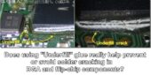
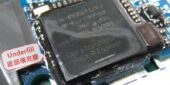
Traditional underfill fills the gap beneath the BGA package and helps distribute mechanical loads across a larger area. For applications where full underfill is not practical, corner bonding or edge bonding may provide additional reinforcement with less material and potentially easier rework. -
Increase the BGA pad size on the PCB. Larger pads may improve pad anchoring or change the solder joint geometry, depending on the pad design. However, larger pads reduce the available routing space between adjacent solder balls and may complicate PCB routing. The effects on solder joint reliability and PCB manufacturability must be evaluated together.
-
Consider SMD (Solder Mask Defined) pad design. In an SMD design, the solder mask overlaps the edge of the copper pad, helping anchor the pad to the PCB. For more details, see Copper Defined vs. Solder Mask Defined pad design for BGA soldering strength.
It is important to understand that SMD and NSMD (Non-Solder Mask Defined) designs each have advantages and disadvantages. SMD pads can improve the mechanical anchoring of the copper pads to the PCB, but may affect solder joint geometry and fatigue performance. NSMD pads generally provide more exposed copper for solder wetting and a different stress distribution, but the copper pads may be more susceptible to pad lift under certain loading conditions. Neither design is universally better; the choice should be based on the package, PCB construction, and expected mechanical loads.
Figcaption: BGA pad layout between SMD and NSMD For further discussion, see:
實驗比較SMD與NSMD焊墊設計推球及拉力測試對BGA錫裂的影響
Should BGA Pads Be Designed as SMD or NSMD? Pros, Cons, and Drop-Test Performance
Experimental Comparison of SMD and NSMD BGA Pad Designs Using Ball Shear and Pull Tests -
Consider vias-in-pad (VIP) design
Vias placed directly within BGA pads can provide routing advantages and may improve certain aspects of pad anchoring, depending on the PCB construction. However, these vias must be properly filled and capped or otherwise processed according to the required design specifications. Unfilled or inadequately processed vias can allow outgassing during reflow, creating voids or other solder joint defects that may weaken the joint and contribute to cracking. For more information, see 【導通孔在墊(Vias-in-pad)的處理原則】.
Related post: Why BGA soldering ball always crack(6)? The recommendation of BGA pad design from workingbear -
Increase solder volume when appropriate
Increasing the solder paste volume may improve certain BGA solder joint conditions, but it is not a universal solution for cracking. Excessive solder can increase the risk of bridging and other assembly defects. Any adjustment should be validated through solder joint inspection and mechanical reliability testing. For more information, see Can Increasing Solder Paste Volume Improve BGA Soldering Defects?.
Validate the Design with Strain Measurements and Simulation
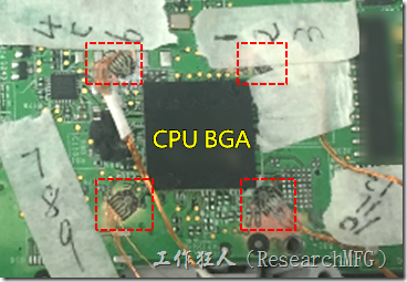
Workingbear strongly recommends that, when investigating an existing product, engineers use strain gauges to identify areas of high PCB strain during critical manufacturing and handling operations. This helps determine where excessive deformation occurs and whether the BGA area is exposed to potentially damaging mechanical loads.
If physical strain measurement is difficult or additional insight is needed, finite element analysis (FEA) can be used to simulate the mechanical behavior of the PCB and enclosure. The simulation can help identify potential stress concentrations and evaluate design changes before building new prototypes.
For a practical example, see 【BGA錫裂,使用應變片(Strain Gauge)量測電路板到底哪個環節產生較大變形量】.

If you are interested in BGA solder joint cracking and component detachment, I also recommend reading the following article: Why Do BGA Solder Balls Keep Cracking (1)? Stress > bonding-force
Related Posts:
- Micro-USB連接器掉落的解決對策
- 板對板連接器(B2B connector)掉落的改善措施
- Solution to Prevent Component Drops During Second Time Reflow Soldering
- Component Drop-Off on PCBs: How to Analyze, Troubleshoot, and Identify the Root Cause
- How to Evaluate the Risk and Probability of Electronic Components Not Falling Off during SMT Second Reflow



Leave a Reply