


Many engineers have asked the same question: When a BGA solder joint cracks or a BGA component falls off the PCB, how can you tell whether the root cause comes from the SMT manufacturing process, the PCB fabrication process, or the product design itself?
Based on Workingbear’s experience, many design engineers immediately assume that any BGA solder crack or component detachment must be caused by poor soldering during SMT assembly. Unfortunately, this often leaves manufacturing engineers with little opportunity to defend themselves because they lack solid evidence proving that the design may actually be the real problem.
From what Workingbear has seen over the years, some BGA failures are indeed caused by manufacturing defects or component quality issues. However, many cases are actually related to PCB layout, mechanical design, or overall product reliability. In fact, solder joint cracking is very often linked to design issues rather than manufacturing.
(This article focuses mainly on manufacturing-related analysis. However, Workingbear later realized that a surprisingly large percentage of BGA solder joint failures are ultimately caused by design problems.)
Start by Understanding When and Where the Failure Occurred
Before analyzing the failure itself, you should first understand the environment in which the failure occurred. The same physical failure can have completely different root causes depending on the operating conditions.
BGA solder cracks or component detachment most commonly occur during impact drop tests, tumble tests, or when customers accidentally drop the product during normal use.
If a solder joint cracks or a BGA falls off without any external mechanical stress, there is about a 99% chance that the problem originated during manufacturing. Typical causes include open solder joints, cold solder joints, poor wetting due to oxidation on either the component or PCB pad, or PCB surface finish problems such as excessive phosphorus content in ENIG plating, which may lead to the well-known Black Pad defect.
Another possibility is that the PCB was bent during manufacturing, leaving residual stress inside the board. That stress may later be released during in-circuit testing (ICT), bed-of-nails testing, or final product assembly, eventually causing the solder joint to crack.
Next, Understand How the Failure Occurred
The next step is to think about a simple question:
Where would the assembly naturally break first?
The answer is obvious—it will fail at its weakest point.
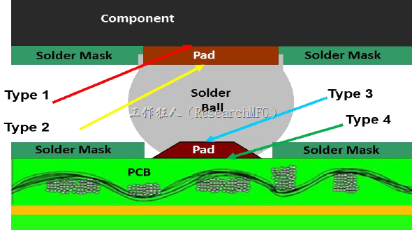
If the failure is caused by poor reflow soldering, the crack will most likely occur between the BGA solder ball and the PCB pad.
Keep in mind that this type of failure may also result from oxidation on either the BGA solder balls or the PCB pads. These conditions commonly produce defects such as Head-in-Pillow (HIP/HoP) or Non-Wet Open (NWO).

If the PCB pad itself is too small to withstand mechanical shock, the impact may tear the copper pad away from the PCB. Of course, pad lifting can also be caused by poor PCB lamination quality.
Another possibility is excessive voiding inside the solder ball. Large internal voids weaken the solder joint and may cause the solder ball to fracture through its center.
Always Examine Both the BGA and the PCB Fracture Surfaces
Because there are many possible failure mechanisms, you should always inspect both sides of the failed joint—the solder ball remaining on the BGA package and the corresponding PCB pad.
Only by examining both fracture surfaces can you determine exactly where the failure occurred.
Besides identifying the fracture location, you should also carefully observe the fracture appearance to determine whether the joint failed because of mechanical overload or poor soldering.
A high-magnification optical microscope is usually the minimum requirement. For more detailed failure analysis, SEM/EDS (Scanning Electron Microscope with Energy-Dispersive X-ray Spectroscopy) is often used to examine the fracture morphology and identify its elemental composition.
What to Look for on the BGA Side
When analyzing a detached BGA, each solder ball should be evaluated together with its matching PCB pad.
Start by checking whether the solder ball is still attached to the BGA package.
Normally, the solder ball should remain on the BGA substrate after failure. If the solder ball is missing from the package, the problem may actually originate inside the BGA package itself.
If the solder ball is still attached, examine the fracture surface.
A rough, irregular fracture surface usually indicates that proper metallurgical bonding occurred and that the joint failed later because of mechanical stress or impact.
On the other hand, if the fracture surface is smooth, shiny, and curved, it is more likely a non-wetting defect or cold solder joint. In these cases, the corresponding solder surface on the PCB pad will usually appear similarly smooth.
If the fracture occurs through the middle of the solder ball, carefully inspect the cross-section for smooth internal cavities. These usually indicate voids inside the solder ball.
Voids reduce the mechanical strength of the solder joint, much like a hollow structural column is weaker than a solid one.
Voids can result from many causes. Some are related to an improperly optimized reflow profile. Others are caused by poor PCB layout decisions—for example, placing vias directly inside BGA pads simply to save routing space. Designers sometimes overlook the manufacturing consequences of this choice, which can lead to insufficient solder, excessive voiding, and poor solder joint reliability, leaving the manufacturing team to deal with the resulting problems.
Related Reading: Design Guidelines for Vias-in-Pad
Workingbear generally does not recommend using vias-in-pad unless the vias are properly filled and plated over.
Years ago, many PCB designers preferred not to specify filled vias because they significantly increased PCB fabrication costs. However, if vias are properly filled and plated, they not only preserve solder quality but can also improve pad adhesion to the FR-4 substrate by acting as mechanical anchors.

Related Reading:
- Should BGA Pads Use SMD or NSMD? Pros and Cons of Each Design
- Differences, advantages, disadvantages, and recommendations for SMD and NSMD pad designs
What to Look for on the PCB Side
Finally, inspect the PCB fracture surface.
If the copper pad has been completely torn away from the PCB, it indicates that the bond between the pad and the PCB laminate was the weakest part of the structure.
Possible causes include undersized PCB pads, insufficient copper-to-laminate adhesion, or weakened bonding caused by repeated high-temperature rework.
Generally speaking, NSMD (Non-Solder Mask Defined) pads use smaller copper pads than SMD (Solder Mask Defined) pads.
Because the solder mask partially overlaps an SMD pad, the copper pad itself must be made larger in order to maintain the same solderable area. As a result, SMD pads usually have stronger adhesion to the PCB laminate than NSMD pads.
What if the fracture occurs along the IMC (Intermetallic Compound) layer? Please refer to the related article:
- Concept Clarification: IMC Layer Fracture Despite the Formation of Effective Solder Joints
- What is IMC (Intermetallic Compound)? How does IMC relate to PCB solder joint strength? Are there IPC standards for IMC thickness?
Consider Underfill Only as a Last Resort
If you’ve exhausted every reasonable design and manufacturing improvement but still cannot solve the reliability problem, then you may consider using underfill glue.
However, underfill should generally be viewed as a last resort. It adds extra dispensing and curing steps after reflow and functional testing, increases manufacturing cost, and makes future repair or rework much more difficult.
Related Posts:
- Red Dye Penetration Test to check for BGA solder joint cracking
- Why BGA soldering ball always crack(1)? Stress > bonding-force
- BGA Cross-Section Analysis: How to Evaluate Solder Joint Quality and Identify Common Defects





Leave a Reply