In this blog, Workingbear has explored the causes and analysis of soldering cracks and electronic component detachment in several articles. It has consistently mentioned that most of the fractures occurring when electronic components detach happen at the Intermetallic Compound (IMC) layer. This indicates that the most vulnerable part of the overall structure, once the component is soldered to the PCB (Printed Circuit Board), is this IMC layer, hence the fractures occurring at this point.
However, nearly all articles also point out that it is essential to form this IMC layer between the solder paste and the component leads, as well as between the solder paste and the metal of the PCB, for effective soldering, ensuring solder joint strength.
Many readers may now start to wonder: if the formation of the IMC layer indicates good solder joint strength, why do fractures almost always occur at the IMC layer after soldering? Isn’t that contradictory?
In fact, this understanding is not contradictory at all. Here, Workingbear attempts to address the most common questions readers may have and provide answers. If any readers have different opinions, please feel free to express them.
Question 1: When the solder forms the IMC layer, it indicates effective soldering confirmation, and the reason for its high soldering strength is because of the high strength of IMC. Why then, during pull and push force tests of solder joints, does the fracture occur from the IMC layer rather than from the middle of the component lead or the solder?
Answer 1: First of all, the formation of IMC during the soldering process is indeed one of the essential criteria for confirming good soldering and soldering strength. However, many people may misunderstand that the term “effective soldering” refers to whether the soldering is good, but it does not guarantee that the solder joint can necessarily withstand more pulling or pushing force than the original joined structure.
Let’s explain this using the analogy of building a wall with bricks and cement. The bricks represent the metal plating of the PCB pads and component leads, while the cement represents the IMC, as it acts to connect the pad and lead. (Note: IMC is actually formed between the solder and the component lead plating, as well as between the solder and the metal of the PCB.)
When two bricks are joined together with cement and undergo external force causing them to break, the cement layer usually cracks first, not the bricks. However, you wouldn’t question, “I’ve applied cement between the bricks, why does it still break from the cement?” Similarly, during the PCB soldering process, the quality of the formed IMC layer indicates higher soldering strength, which refers to effective soldering, and this is the source of the IMC layer’s ability to withstand higher pull and push forces.
However, why the solder joint always seems to fracture from the IMC layer when subjected to external force is another matter. Solder joint fractures always begin at the structurally weakest point, just like a dam collapses from its weakest point. Knowing where the solder joint fractures occur requires analyzing the maximum force each part of the solder joint can withstand when subjected to external force.
Because IMC is an intermetallic compound formed by the combination of two or more metals, its ability to withstand shear stress is generally weaker than that of pure metals. Hence, solder joint fractures almost always occur at the IMC layer. This is analogous to a child being the weakest link between a boy and a girl holding hands.
If you’re still unsure, check out this article of “What is IMC (Intermetallic Compound)? How does IMC relate to PCB solder joint strength? Are there IPC standards for IMC”, or watch Workingbear’s YouTube video explaining what IMC (Intermetallic Compounds) is and why they are inevitable in soldering.
Question 2: When conducting solder pull tests, after the component is pulled off, we often see a layer of white or gray material on the fracture surface, which many say is the IMC layer. But where exactly does the IMC layer form?
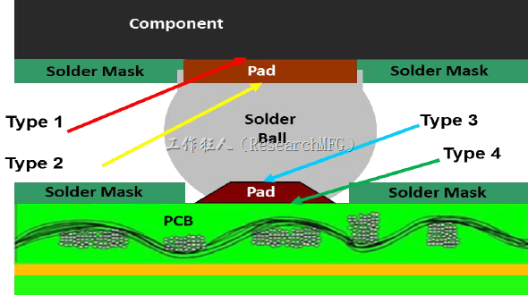
Answer 2: Please refer to the diagram at the top of the article. In fact, both points A and B in the picture can form the so-called “IMC layer.” Additionally, there is also a small amount of various IMCs present within the solder paste. However, because the vast majority of the solder paste is composed of “tin,” even if IMC is formed and mixed within it, it will be diluted and not easily detectable. However, with careful observation, IMCs like AuSn4 (dot-shaped) and Ag3Sn (strip-shaped) that wander in the solder can still be seen.
As for the IMC at points A and B, it depends on the surface finish of the material to determine what type of IMC compound will be formed. If it’s a “copper” based PCB surface finish, such as OSP (Organic Solderability Preservatives), I-Ag (Immersion Silver), I-Sn (Immersion Tin), or HASL (Hot Air Solder Leveling), it will mostly form Cu6Sn5 IMC. If it’s a “nickel” based PCB surface finish, such as ENIG (Electroless Nickel Immersion Gold), ENXG, or ENEPIG, it will generate benign Ni3Sn4 IMC.
Different metals combined with tin will produce different IMCs.
Related Reading: What are “copper” and “nickel” based Printed Circuit Boards (PCBs)?
Question 3: In normal solder pull tests, which IMC layer, A or B, is most likely to fracture?
Answer 3: This question comes down to explaining the stress each part of the solder joint can withstand. As mentioned in Answer 2, the IMC layer is generally the weakest point in the entire solder joint. However, there are usually two IMC layers in the solder joint. So, which layer, A or B, is more likely to fracture?
Assuming the force applied and the force point are the same, and the contact area of the solder is also the same, without other interfering factors, it depends on the type of IMC formed. Generally, the IMC formed on “copper” bases is stronger than that on “nickel” bases. However, the IMC on “copper” bases tends to gradually age over time, making the IMC layer brittle.
Therefore, if a component lead plated with nickel and then coated with tin is soldered onto a PCB with ENIG surface treatment (“nickel” base), it is more likely to fracture from position B.
If a component lead plated with nickel is soldered onto a board with OSP surface treatment (“copper” base), it is more likely to fracture from position A.
If a component lead plated with nickel and then coated with tin is soldered onto a PCB with OSP surface treatment (“copper” base), it’s a toss-up. In this case, it depends on which side has the more intact IMC or a larger area.
Recommended Reading: Comparing the solder joint strength of PCBs with OSP and ENIG surface finishes.
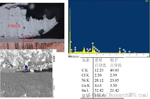
The image below shows a sliced element analysis report of a component drop on an ENIG finished PCB. Take a look for yourself!

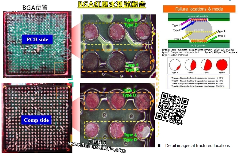
Please note: The above explanation may not apply well to BGA soldering, as BGA soldering also depends on the design of its pads as SMD or NSMD, which will affect the strength of the solder structure.
Recommended Reading: To prevent solder ball cracking, should BGA pads be designed as SMD or NSMD? Pros and cons of SMD and NSMD.
Related Posts:


Leave a Reply