Working for manufacturer engineering couple years. Sharing the manufacturing experience, skill, DFx, design, and information. Be care of this blog is personal share and content may not be 100% correctly.
Lately, many colleagues have been asking WorkingBear for advice on designing BGA (Ball Grid Array) packages to prevent solder joint cracking and improve overall durability. This sudden interest came after a senior manager raised concerns during a new product development meeting, warning that if customers continue reporting BGA cracking issues, someone will be held accountable.
The real problem, however, stems from unrealistic expectations at the executive level. Leadership wants products to be thinner, lighter, and completed faster—shrinking the development timeline from 12 months to 9, and now just 6. At the same time, they expect flawless design execution with zero delays. Under this pressure, engineers are pushing themselves to the limit, often at the cost of their health. It’s worth asking: how did our company culture end up like this?
WorkingBear has covered topics like BGA drop damage, soldering defects, and solder ball cracking in previous blog posts. However, there hasn’t been a comprehensive summary of how to strengthen BGA designs specifically to prevent cracking—until now.
Before we dive into design strategies, it’s important to understand why BGA solder joints crack in the first place. Let’s assume proper soldering and ideal intermetallic compound (IMC) formation—yet cracking still occurs. In most cases, the root cause is mechanical stress. Based on WorkingBear’s analysis of real-world failures, nearly all cases of BGA detachment or cracking can be traced back to stress acting on the PCB.
There are several sources of stress that cause components to drop from PCB or soldering crack on a board.
Internal creep generates stress: For instance, during reflow, the printed circuit board (PCB) or BGA substrate may deform at high temperatures, and stress is continuously released until it reaches an equilibrium point, which could lead to solder balls cracking.
External impact or pressure creates stress: For instance, mobile phones may bend while in a user’s pocket (similar to the iPhone 6 Plus “bendgate” incident) or experience impact stress when accidentally dropped on the ground.
Thermal expansion and contraction due to changes in environmental temperature causes stress: In some areas, outdoor temperatures can freeze in the winter, causing rapid temperature changes when products are moved from a heated indoor environment to the frozen outdoors. In tropical regions, the indoor environment may be cooled with air conditioning, causing significant temperature changes when moving outdoors. Additionally, placing products in a car can cause temperature changes from daytime heat to nighttime cooling. Temperature is critical since different materials have different coefficients of thermal expansion (CTE), and the CTE of the PCB material is undoubtedly different from that of the solder balls and BGA substrate material. To reduce the risk of material expansion and contraction, electronic component materials rely on using materials with smaller differences in CTE, much like roads and bridges have expansion joints.
Once we understand that BGA components falling off or solder balls cracking are closely related to stress, we can discuss ways to strengthen the BGA’s design and prevent cracking as much as possible. Methods are only valuable if they are implemented, so it depends on whether or not to implement them. There are two orientations to consider:
First, finding ways to reduce stress impact.
Second, strengthening the BGA’s ability to resist stress.
Here are several methods to enhance the BGA’s resistance to cracking:
1. Enhance PCB’s resistance to deformation
PCB deformation typically results from the rapid heating and cooling caused by high-temperature reflow, combined with heavy components and unevenly distributed copper foil on the PCB, which worsens the deformation.
Methods to increase PCB’s resistance to deformation include:
Increase PCB thickness. If possible, use a PCB with a thickness of 1.6mm or more. If you must use a board with a thickness of 0.8mm, 1.0mm, or 1.2mm, use a reflow carrier to support PCB and strengthen the board and prevent it from deformation during reflow.
Use high Tg PCB material. A high Tg means high rigidity, but the price also increases, so this must make trade-offs.
Add reinforcement ribs around the BGA. If there is space, consider adding supporting metal frames around the BGA to enhance its ability to resist stress, like building a house.
Potting epoxy resin onto the PCB. It is also possible to consider dispense glue around the BGA or on the back of the corresponding PCB to strengthen its ability to resist stress.
2. Reduce PCB deformation
In general, Once a PCB is assembled into a casing, it should be protected by the casing. However, because today’s products are getting thinner, especially handheld devices, PCB deformation often occurs due to external bending or impact caused by drops.
To reduce the deformation caused by external forces on the PCB, the following methods can be used:
Increase the buffering design of the structure on the PCB. For example, design some buffering materials, so that even if the casing is deformed, the internal PCB can still be protected from external stress. However, the service life and capacity of the buffering materials must be considered.
Add screws or positioning fixed structures around the BGA. If our goal is only to protect the BGA, then we can forcibly fix the structure near the BGA to prevent deformation near the BGA.
Strengthen the casing strength to prevent its deformation from affecting the internal PCB.
3. Enhance the fastness of BGA
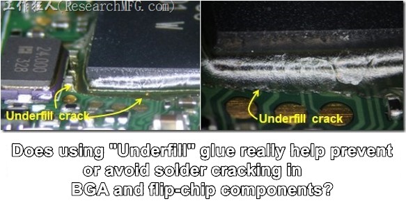
Dispense “Underfill” glue at the bottom of the BGA.
Enlarge the size of the BGA solder pads on the PCB. This will enhance pad bonding strength on the PCB. But this also makes wiring on the PCB more difficult because the space between the balls for signal routing is reduced.
※Note: The SMD and NSMD pad designs actually have their respective advantages and disadvantages. Adopting SMD can enhance the bonding strength between the solder pads and the PCB, but it is not conducive to the solder joint strength of the solder balls. Adopting NSMD will enhance the solder joint strength, but it is not conducive to the bonding strength between the solder pads and the PCB.
Use Vias-in-pad (VIP) design. However, the via holes on the solder pads must be filled with copper electroplating to prevent soldering voids during reflow, which can cause the solder balls to break in the middle. This is similar to the idea of anchoring a house with ground screws to prevent seismic damage.
Related post: Why BGA soldering ball always crack(6)? The recommendation of BGA pad design from workingbear
Increase the amount of solder volume. It is noting help to strengthen the solderability for BGA ball. Increasing the solder volume is in order to reduce the HIP/HoP of soldering defect. However, it should be ensured that this increase does not result in soldering short.
For those who have a finished product, WorkingBear strongly recommends using a Strain Gage to locate the stress concentration point of the circuit board. In case of difficulties, one can also consider using a computer simulator to identify potential areas of stress concentration.


 still cannot screen out the DDR soldering fail?")
 Explained: A Complete Guide to New Product Development in Electronics Manufacturing")

? Stress > bonding-force")


Leave a Reply