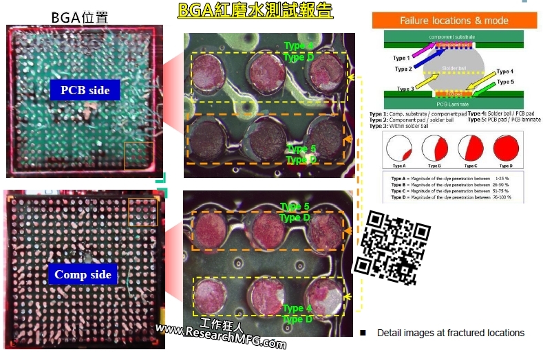
 Improving the solderability of BGA (Ball Grid Array) packages is always a big challenge for the SMT (Surface Mount Technology) process. Fine pitch BGAs (with a ball pitch less than 0.8mm) are particularly difficult to solder onto the PCB. Additionally, inspecting the soldering result is challenging because the solder joints are hidden under the BGA body, and sometimes even 2D X-Ray inspection is insufficient. (5Dx or angle rotation X-Ray might be able to inspect BGA soldering quality, but these methods are expensive.)
Experience tells us that most BGA solderability failures are caused by the HIP (Head-In-Pillow) or call HoP (Head-on-Pillow) soldering defect, and over 90% of HIP defects occur at the four corners of the BGA package. This is due to the longer diagonal distance and the greater impact from board warpage and BGA deformation. Many senior SMT engineers have conducted experiments and proven that increasing the solder paste volume on the pads under the BGA can reduce the risk of HIP defects.
Below is an idea on how to partially increase the solder paste volume under a BGA without increasing the solder paste volume for all balls. Be careful not to apply too much solder paste, as this can cause solder shorts.
Workingbear modifies the stencil aperture size for BGA packages to control the solder paste volume. Ideally, the outer rows of the BGA balls should have more solder paste volume, while the inner BGA balls should have less solder paste. This is because HIP defects typically occur at the four corners of the BGA and rarely appear in the inner rows of BGA balls.
 |
|
The pictures below show a BGA with ball sizes less than 0.4mm in diameter and using the circumscribed circle pad method. As a result, you will notice that the ball sizes on the four sides of the outer row are larger than the others.


Below picture shows the actual stencil aperture result for BGA package with ball sizes less than 0.4mm in diameter.

Related Posts:


Leave a Reply