
The Intermetallic Compound (IMC) layer grows in the interface between Cu-based, Ni-based and Sn-solder is the certain result of the chemical reaction that forming the soldering joint. But the IMC layer is also the weakest location of the solder bonding-force.
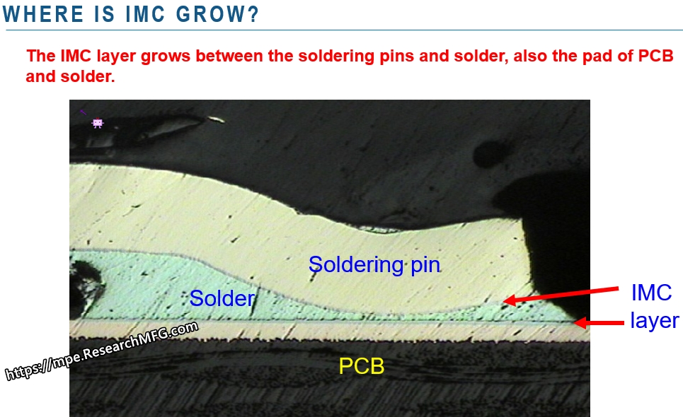
As mentioned last page, the bonding strength of PCBA shall include a minimum of 5 defect positions. Identifying the growth of IMC is crucial in determining the quality of soldering. If there is no IMC layer grows between the solder alloy and Cu or Ni substrate, the electronic component and PCB will not be joined. However, the IMC layers are also the weakest point in the whole soldering strength structure. Why?
The IMC is the abbreviation of Inter-Metallic Compounds in the electronics manufacturing industry. The IMC layer is the certain result of the chemical reaction to form the soldering joint. WorkingBear likens the IMC layer just like a child born from the marriage of a girl and a boy.
As workingbear previously mentioned, the “IMC layer is like the cement applied between bricks to construct a wall”. The proper application of right amount of cement and even coating it can ensure the strongest bond between the bricks, but excessive or uneven cement application can cause the wall to collapse easily. Similarly, the IMC layer is critical to forming a strong solder joint, but it is also the weakest layer in the soldering structure. When considering where a brick wall would break if struck with a hammer, most cracks would occur in the cement layer. Similarly, stress on the solder joint would first impact the IMC layer, just as it would with the cement layer.
If you still do not fully understand what IMC is, it is recommended that you read the article on “[What is IMC (Intermetallic Compound) in the electronic manufacturing industry?] ” first.
Here comes a video to introduce what is the IMC.
Therefore, can poorly applied or uneven cement, or a layer that is too thick or thin, affect the bonding strength of the soldering? The answer is yes. If solder cracks occur at the IMC layer, the continuous and even growth of the IMC layer between the metal interface must be checked. Engineers typically use cross-sectioning or call micro-sectioning and Scanning Electron Microscope (SEM) to examine the IMC growth status and Energy Dispersive X-ray Spectrometer (EDX) for elemental analysis and chemical characterization for further evaluation.
Generally, uneven or discontinuous IMC growth is rare unless the reflow or soldering process did not provide enough thermal energy or if there is oxidation on the PCB pad finish and component solder terminals.
While IMC layer growth that is too thick or too thin can affect the strength of the solder bonding force, there is nothing the SMT process can do to improve it. What the SMT process can do is promote even IMC layer growth between the metal interface. This is because once the IMC layer grows, its thickness will increase over time and with heat accumulation. When the IMC layer becomes too thick, the soldering strength will decrease, becoming more brittle. This is similar to the cement applied between bricks. The correct amount of cement can strongly bond different bricks together, but if the cement layer is too thick, it can easily be pushed down. This also explains why the reliability of electronic products worsens over time.
No mater the IMC layer growth too thick or too thin can affect the strength of solder bonding-force, there is nothing the SMT process can do to improve it. What SMT process can do is to promote even IMC layer growth between the metal interface. This is because once the IMC layer grows, its thickness will increase over time and with heat accumulation. When the IMC layer grows too thick, the soldering strength will become worse and brittle. This is similar to the cement applied between bricks. The correct amount of cement can strongly bond different bricks together, but if the cement layer is too thick, it can easily be pushed down from the cement layer. This also explains why the reliability of electronic products worsens over time.
There are many people keep chasing Workingbear what the ideal thickness of the IMC layer is. Workingbear suggests that the best thickness of the IMC layer should be 1-3um, but the regular acceptable thickness for Copper-Tin (CuSn) and Copper-Nickel (CuNi) intermetallic compounds is 1-5um.
There is a factor in the SMT process that needs to be taken care of, which is the voids in the solder joints. These voids have a deleterious impact on the reliability of solder joints because they weaken the strength of the solder joint. Most of the voids typically contain nothing but air, while some may contain flux residues or cured resins when epoxy glues or resin-containing pastes are used. These voids are trapped gases (air, humidity, or chemical ingredients of fluxes) within the joint that had insufficient time to escape during the reflow process when the solder is molten and solid.
Two obvious features can help to identify whether the voids came from the air-traps:
1. The inner surface of the voids are smooth.
2. The voids show round shape in the solder joint.
The larger the void, the more unfavorable the soldering strength. How can the hollowed-out wood be able to withstand folding & bending? Unfortunately, the voids in the solder joint are difficult to avoid completely during the soldering process, especially the BGA, QFN, LGA kind of package need a large volume of solder. Since the voids in solder joints can’t be eliminated then think differently to define how many voids or its size can be acceptable at a certain ratio. Once there is better technology then tighten this specification will be ok. It is a trade-off.
According to the requirements of IPC-7095B and IPC-A-610D, the diameter of the total voids of the BGA solder ball can not exceed 25% of the total diameter of the solder balls. Most electronics factories also follow this used to determine the yield of the voids. The specification may be updated in the future and please refer to the latest IPC specifications.

Therefore, only when the IMC cannot grow or the IMC layer didn’t distribute evenly will be correlative with the quality of the SMT process. These may be related to insufficient thermal energy in the reflow oven and may be related to the poor surface treatment of the PCB or the storage environment, or it may be related to the quality of the electronic components. This requires cross-section and elemental analysis solution to provide evidence and judgment.
Now you will be be an expert for the soldering strength now. You shall do your personal analysis and judgment first next time while you meet the soldering crack.
Article series :
- Why BGA soldering ball always crack(1)? Stress > bonding-force
- Why BGA soldering ball always crack(2)? The composition of PCBA bonding-force
- Why BGA soldering ball always crack(4)? Using “copper” base material as the surface finish for PCB
- Why BGA soldering ball always crack(5)? Increase the contact area of solder to increase its strength
- Why BGA soldering ball always crack(6)? The recommendation of BGA pad design from Workingbear
- Why BGA soldering ball always crack(7)? The Bonding force between solder pad of copper foil and PCB substrate
- Why BGA soldering ball always crack(8)? Increase PCB stiffness to resist stress and avoid board bending
- Why BGA soldering ball always crack(9)? Increase the resistance of components to stress
- Why BGA soldering ball always crack(10)? Reduce the impact of PCB bending through the mechanism design change
- Why BGA soldering ball always crack(11)? Stress is the Biggest Culprit in Causing BGA Solder Joint Cracks
- Why BGA soldering ball always crack(12)? Manufacturing Processes That May Generate Significant Stress
- Why BGA soldering ball always crack(13)? Usage Environment is the Biggest Challenge of Stress Sources
Related article:
Increase solder paste volume will improve the MLCC capacitor broken?
 in the electronic manufacturing industry?")
? The composition of PCBA bonding-force")
? How does IMC relate to PCB solder joint strength? Are there IPC standards for IMC thickness?")
? Using \"copper\" base material as the surface finish for PCB")


Leave a Reply