
The earlier sections of the article that Workingbear spent a lot of time discussing how to strengthen the bonding force of PCBAs and increase the stress resistance of electronic products. Now, we can finally talk about the biggest culprit causing BGA solder joint cracks: stress.
To completely solve the problem of BGA solder joint cracks, we must understand where stress comes from and treat it accordingly to avoid or reduce its impact. Without addressing stress issues, all other efforts will only be half as effective, just like managing floodwaters – clearing them is always more effective than building barriers.
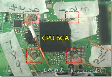
Stress can be divided into two types: internal stress and external stress. Internal stress belongs to the long-term reliability problem of creep, which is not discussed in this article. Only external stress is discussed. Stress is actually everywhere for solder joints, and its greatest impact on solder joint cracks is causing “board bending”. In the early days, PCB thickness was designed to be above 1.6mm, and electronic components were relatively large and robust, so the bending stress caused by assembly was within the range that could be tolerated. However, with the popularity of mobile phones, PCB thickness has become thinner and thinner, and too thin boards can be bent with just a little force. In addition, the diameter of BGA solder balls is also getting smaller and smaller, making their ability to withstand stress worse. Fortunately, technology has also developed with the times.
Now, we can use computer-aided design (CAD) to simulate how stress works on PCBs to cause board bending. However, simulations require inputting many assumptions, so the results usually differ somewhat from reality, but they can still be used as a reference. After the PCB is actually made, strain-stress gages can be used to measure the actual stress that the PCB withstands under various assembly conditions.
Therefore, if your company’s products frequently encounter problems such as BGA solder joint cracking or MLCC capacitor cracking during production, Workingbear strongly recommends using strain-stress gages to measure the actual stress caused by various assembly and testing processes and then improving processes that exceed stress limits.
Article series :
- Why BGA soldering ball always crack(1)? Stress > bonding-force
- Why BGA soldering ball always crack(2)? The composition of PCBA bonding-force
- Why BGA soldering ball always crack(3)? IMC layer growth is a certain result to form the soldering joints
- Why BGA soldering ball always crack(4)? Using “copper” base material as the surface finish for PCB
- Why BGA soldering ball always crack(5)? Increase the contact area of solder to increase its strength
- Why BGA soldering ball always crack(6)? The recommendation of BGA pad design from Workingbear
- Why BGA soldering ball always crack(7)? The Bonding force between solder pad of copper foil and PCB substrate
- Why BGA soldering ball always crack(8)? Increase PCB stiffness to resist stress and avoid board bending
- Why BGA soldering ball always crack(9)? Increase the resistance of components to stress
- Why BGA soldering ball always crack(10)? Reduce the impact of PCB bending through the mechanism design change
- Why BGA soldering ball always crack(12)? Manufacturing Processes That May Generate Significant Stress
- Why BGA soldering ball always crack(13)? Usage Environment is the Biggest Challenge of Stress Sources
Related article:
Increase solder paste volume will improve the MLCC capacitor broken?
? The recommendation of BGA pad design from workingbear")
? The composition of PCBA bonding-force")
? Stress > bonding-force")
? Usage Environment is the Biggest Challenge of Stress Sources")
? Increase PCB stiffness to resist stress and avoid board bending")
? Reduce the impact of PCB bending through the mechanism design change")


Leave a Reply