How to increasing the ability of components to resist stress?(Continuing from the previous article)
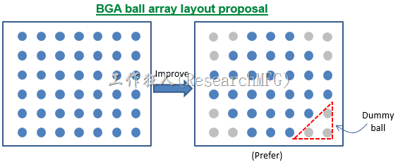
2. No solder balls on BGA four corners, or use dummy balls instead of them.
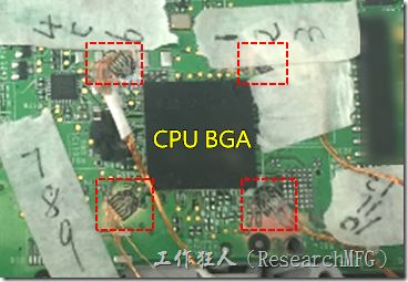
If you had studied the actual phenomenon of BGA solder cacking under a microscope, you should find that most BGAs start to break from the solder balls at the four corners. This is because the four corners of the BGA have the farthest distance from the force moment of the board bending, so they are also the positions that sustain the maximum stress during the board bending and warping, and of course, are the most likely to cause solder ball fractures.

Therefore, in the design of BGA packaging, if you can design dummy balls without functional signals or simply do not has balls in the four corners, it can effectively protect the solder joints at the four corners of the BGA and reduce the cracking risk of solder ball. Many SRAM and DDR BGA packaging now use this design, but in my opinion, CPUs and MCUs should be the BGAs that most need to introduce this design because they have the largest size.
3.Use a reflow carrier or full-process carrier to reduce the risk of board bending & deformation for thinner PCBs.


If the thickness of the PCB is below 1.2mm, a “reflow carrier” should be used. If it is below 1.0mm, a “full-process carrier” strongly be necessary. Even for boards with a thickness of 1.6mm or more, the use of an SMT carrier may depend on its situation.
The main purpose of using an SMT carrier is, of course, to reduce and prevent PCB bending and deformation. Once the PCB is deformed, it will bear additional bending stress in subsequent testing and assembly processes because all fixture designs assume that the PCB is flat. When using the fixture for testing, the fixture will actually apply stress to keep the PCBA back to flatness. Moreover, a PCB that is bent and deformed is very unfavorable for soldering large components, especially for BGAs and LGAs, because their solder will be elongated and thinned or compressed and fattened, reducing their ability to withstand stress.
Recommended reading: When does SMT require Reflow Carriers and Full Process Carriers?
Why PCBs will bend and deform during reflow process? Because lead-free PCBs use the Tg150 substrate only, meaning that PCB will change to rubbery state and become soft and flexible above its Tg value (150°C).
However, the reflow temperature of the lead-free process is as high as around 250°C, which means that today’s PCBs will inevitably undergo some degree of deformation after passing through the reflow oven. Moreover, the thinner the PCB, the more severe the softening deformation will be in the reflow oven. Of course, other factors may also affect the board bending, such as the uniformity of copper foil distribution on the board, the presence of heavy components, the size and location of the board, the size of the connecting ribs in the laminate, and so on. Temperature is the biggest contributing factor, and using a carrier can force the PCB to keep its flatness during it running in reflow oven and reduce the amount of board bending deformation.
Workingbear must be emphasized that “although using a carrier can effectively suppress PCB deformation, it cannot absolutely solve the problem of BGA solder joint cracking”. If your board thickness is already below 0.8mm, to be honest, it may bend even at normal temperatures, and one careless operation can cause solder joint cracking, which is really troublesome. In addition, not only PCBs, but also carrier plates on BGAs can be warped or bent. Although high Tg materials are used for the carrier plate, the maximum Tg is only Tg175, and poorly designed BGAs may bend like bananas during reflow.
It can be said that “R&D engineers make mistake, the process engineers deal with the sequences.”
Recommended further reading: What is Tg (Glass Transition Temperature) and Its Role in PCBs?
Article series :
- Why BGA soldering ball always crack(1)? Stress > bonding-force
- Why BGA soldering ball always crack(2)? The composition of PCBA bonding-force
- Why BGA soldering ball always crack(3)? IMC layer growth is a certain result to form the soldering joints
- Why BGA soldering ball always crack(4)? Using “copper” base material as the surface finish for PCB
- Why BGA soldering ball always crack(5)? Increase the contact area of solder to increase its strength
- Why BGA soldering ball always crack(6)? The recommendation of BGA pad design from Workingbear
- Why BGA soldering ball always crack(7)? The Bonding force between solder pad of copper foil and PCB substrate
- Why BGA soldering ball always crack(8)? Increase PCB stiffness to resist stress and avoid board bending
- Why BGA soldering ball always crack(10)? Reduce the impact of PCB bending through the mechanism design change
- Why BGA soldering ball always crack(11)? Stress is the Biggest Culprit in Causing BGA Solder Joint Cracks
- Why BGA soldering ball always crack(12)? Manufacturing Processes That May Generate Significant Stress
- Why BGA soldering ball always crack(13)? Usage Environment is the Biggest Challenge of Stress Sources
Related article:
Increase solder paste volume will improve the MLCC capacitor broken?


Leave a Reply