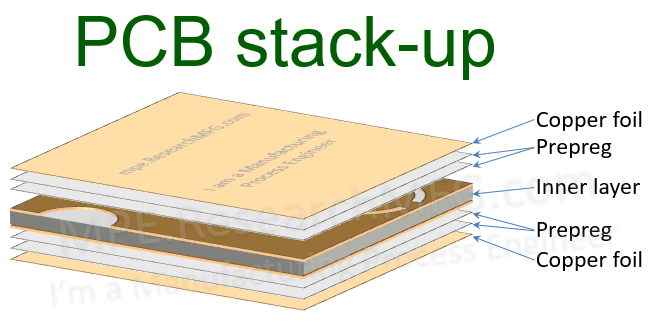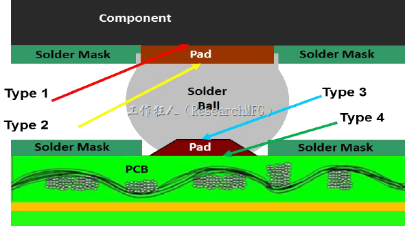
PCB is composed of layers of Copper Clad Laminate (CCL) and Prepreg (PP) stacked together. In modern PCB manufacturing, CCL has become a standard material. Each CCL manufacturer provides customers with product specifications that indicate the peel strength of the CCL. From these specifications, we can see that the peel strength is higher when using 1.0 oz copper foil thickness than when using 0.5 oz. Different models and manufacturers of CCL also have different peel strengths, so selecting the appropriate CCL specifications is necessary to enhance the bonding force between the copper foil and PCB substrate.

What is Copper Clad Laminate (CCL)?
With the evolution of manufacturing technology and industrial specialization, Copper Clad Laminate (CCL) has become one of the standard materials used in the manufacturing production of Printed Circuit Boards (PCBs). In the early days, PCB manufacturers had to paste copper foil onto the insulating substrate themselves, but this is no longer necessary.
Copper Clad Laminate (CCL) is a type of material used in printed circuit boards (PCBs) that consists of a layer of copper bonded to a non-conductive substrate, typically made of fiberglass or paper impregnated with resin. The copper layer is etched away in a specific pattern to create the conductive pathways that form the circuits.
The purpose of CCL in PCBs is to provide a stable and conductive surface on which the electronic components can be mounted and interconnected. The copper layer serves as the conductive material that allows electricity to flow through the PCB, while the non-conductive substrate provides insulation to prevent short circuits and interference between the circuits.
The PCB substrate is basically composed of the following four materials:
- Copper foil
- Reinforcement
- Resin matrix
- Fillers system
The copper foil is used for power layers, ground layers, and electronic signal transmission layers, while CCL is uniformly coated with a layer of copper foil on a hard insulating substrate. The thickness of the insulation layer and copper foil generally follows standard specifications based on customer requirements, but can also be customized. CCL can be classified into single-sided copper foil and double-sided copper foil according to the needs.
Recommended reading: Introduction to the structure, characteristics and precautions of Printed Circuit Board materials

Modern PCB manufacturers only need to select the required CCL based on the Gerber file provided by the customer, etch the circuit on the CCL copper foil, and then apply a PP film between adjacent CCLs to prevent short circuits between different CCL copper foil layers that should not occur. The layers are then connected by via holes (similar to connecting stairs in a building) to complete the PCB.
Recommended reading: Why are there holes in circuit boards? What are PTH/NPTH/vias?
Classification of CCL
CCL (Copper Clad Laminate) is generally classified into different grades and applications based on the type of base material used. PCB base materials are divided into three main categories: paper-based substrates, composite substrates, and FR4 substrates, each with different characteristics and uses.
“Paper-based substrates (FR-1, FR-2)” are made of phenolic resin and kraft paper. They have a lower grade and their biggest advantage is their low cost and cheap price. However, their structural strength is weaker and they can only be made into single-layer printed circuit boards. Paper-based substrates are widely used but mainly for products with simple circuits and lower technological levels, such as remote controls, TVs, radios, computer keyboards, etc. Most of the printed circuit boards used in these products are made from paper-based substrates.
“Composite substrates (CEM series)” use epoxy resin as the raw material and reinforcement material such as glass fiber cloth and kraft paper or glass fiber paper. They have higher strength than paper-based substrates and can carry heavier weight. However, due to their durability and price being in an awkward range, composite substrates are used less frequently and mainly in video game consoles and computer monitors larger than 17 inches.
As for “FR-4 substrates”, they are currently the highest grade among copper-clad laminates. The resin used is epoxy resin, and the reinforcement is made of multilayer glass fiber cloth (GF) that is tightly pressed. FR4 substrates are commonly used in computer, mobile phones, and peripheral equipment, such as computer motherboards, hard drives, mobile phone motherboards, and other products that use printed circuit boards made from FR4 substrates.
Note: FR is the abbreviation for “Flame Retardant”, indicating that the material meets the UL94V-0 standard. The name FR-4 was created by NEMA in 1968.
Article series :
- Why BGA soldering ball always crack(1)? Stress > bonding-force
- Why BGA soldering ball always crack(2)? The composition of PCBA bonding-force
- Why BGA soldering ball always crack(5)? Increase the contact area of solder to increase its strength
- Why BGA soldering ball always crack(6)? The recommendation of BGA pad design from workingbear
- Why BGA soldering ball always crack(8)? Increase PCB stiffness to resist stress and avoid board bending
- Why BGA soldering ball always crack(9)? Increase the resistance of components to stress
- Why BGA soldering ball always crack(10)? Reduce the impact of PCB bending through the mechanism design change
- Why BGA soldering ball always crack(11)? Stress is the Biggest Culprit in Causing BGA Solder Joint Cracks
- Why BGA soldering ball always crack(12)? Manufacturing Processes That May Generate Significant Stress
- Why BGA soldering ball always crack(13)? Usage Environment is the Biggest Challenge of Stress Sources
Related article:
Increase solder paste volume will improve the MLCC capacitor broken?


Leave a Reply