
As the career of Manufacturing Process Engineering(MPE), WorkingBear has noticed a constant battle between Designers, Marketers, and Manufacturers. Marketers always want thin, modern design that look thin. Designers think fabrication is simple, while Manufacturers want strong, robust, sturdy assemblies that won’t be scratch easily on the surface. However, both of parties also want low costs.
This leads to two common questions from R&D and marketing professionals:
- Why do thinner PCBs require a special carrier or template for the reflow process?
- Aren’t all PCBs reflowed as a panel, requiring a support fixture for de-panelization?
Since WorkingBear is MPE, so I will answer these two questions as manufacturing point.
1. Why do thinner PCBs will require a special carrier or template for the reflow process?
To answer this question, we must first understand that current lead-free PCBs often use TG150 resin. However, the peak temperature of RoHS reflow heats up to around 240°C to 250°C, which means that the PCB will become rubbery when it enters the high-temperature zone of the reflow oven. Additionally, there are many components already located on the PCB, which adds weight and creates a force of gravity that can cause the PCB to deform. The thinner and lower TG resin of the PCB, the worse the deformation. If the PCB thickness is less than 1.0mm, the deformation will become serious. Therefore, WorkingBear recommends applying a 1.6mm thickness of PCB if there is no space concern.
According IPC-A-610, section 10.2.7 of Laminate Conditions – Blow and Twist, defines the PCB deformation or warpage after solder shall not exceed 1.5% for through-hole and 0.75% for surface mount printed board applications. WorkingBear would like to say the PCB warpage is really critical for the PCB Assembly quality, especially when there is a BGA package on board. It is easily to bring the Head-In-Pillow (HIP) or call Head-on-Pillow soldering defect, which WorkingBear will introduce at later time. . You can refers to this article of Why Burn/In(B/I) still cannot screen out the DDR soldering fail? first.
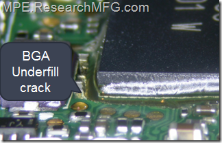
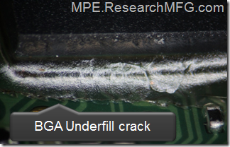
Another concern with thinner PCBs is Underfill crack, which is shown in the two pictures at the beginning of this article. The Underfill around and under the BGA was cracked, and in one case, the PCB with only 1.0mm thickness cracked after a drop test from a height of 120 cm. The drop test deformed the plastic case, warped the PCB, and broke the Underfill glue and ball solder for the BGA.
So, if RD insists on using a thinner PCB, what can be done? One solution is to use a reflow carrier or template made by allium alloy material or composite stone material. The reflow carrier has alignment pins designed according to the actual NPTH (Non-Plating Hole) location on the panel PCB, and it can withdraw higher temperature and be re-cycled for use. I helps to support the PCB and keep it from bending too much.
If reflow carrier is a must fixture to support the thinner PCB in the reflow then it will need about 30~50 pcs quantity to keep the SMT production running smoothly. You must calculate how quantity of reflow carrier will be inside the reflow same time, how many carrier will be buffer to move them from after reflow to before reflow zone. If the PCB thickness is thinner (0.8mm, 0.6mm or FPC) and them can’t be kept flatness on the solder paste printing or pick & place stage then the carrier quantity will be increased to about 60~80 pcs. Because the carrier will be applied from solder paste printing, pick & place, reflow, AOI process. As experience show the reflow carrier may cost you about US100~US200 per unit.
2. Aren’t all PCBs reflowed as a panel, requires a support fixture for de-panelization?
Here we must understand the SMT process flow,as following steps. Please reflow to How EMS fabricate a PCB Assembly? for detail information:
Step 1, Bare board loading into SMT production line
Step 2, Solder paste printing
Step 3, Solder Paste Inspection (Option)
Step 4, Pick and place speed machine
Step 5, Pick and place general machine (low speed)
Step 6, Hand place component and visual inspection (Option)
Step 7, Reflow
Step 8, Auto Optical Inspection (Option)
Step 9, Unloading PCB Assembly (SMT finessed)
Step 10, Visual Inspection
Step 11, Touch-Up (Option)
Step 12, In-Circuit Test
Step 13, Board level Function Verification Test
Step 14, PCB Assembly de-panel
Yes, almost all PCBs are reflowed as panels and require a support fixture for depanelization, but there are two different types of carriers: reflow carriers and depanelization vacuum carriers. Please note that the depanelization vacuum carrier is only used for a router machine to remove the break-away from the panel PCB. If the PCB design has a V-cut and a scoring machine is applied, there is no need for a depanelization carrier.
The reflow carrier is designed to prevent PCB deformation during reflow and must be able to withstand high temperatures and be durable. Therefore, it is made of metal alloy or higher Tg resin.
The depanelization carrier is designed to hold the PCB in place during the milling cutter’s removal of the break-away or connection ribs between board to board. The depanelization carrier also needs to be connected to a vacuum system to remove unnecessary break-away material from the panel board.
Related Articles:


If the PCB is 1.0mm thickness, what’s the point of judgment suggestion to use the fixture in SMT or not ?
Is It still a confidence reliability spec of watching the warpage about 1.5% and 0.75% (user’s filed issue?)
( For a NB or 3C product )
Jimi;
I do think the acceptable criteria for the PCB warpage rate shall base on the actual requirement. Especially for the BGA and MLCC and other bending sensitive components. The IPC standard will be the minimum requirement only. Some products must be survivor after tumbler test and impact test but some desktop products don’t have drop test requirement. It is hard to define the PCB warpage rate for all products.
The warapged PCB is not only affect to the PCBA reliability but also affect to SMT yield rate. The PCB go 1st reflow will be warpaged then 2nd reflow will be a problem.
I only can say the 0.75% is general requirement and most of the PCB fabricator follow it. If you ask smaller warpage rate for PCB then the cost may be raised.