 Many FPCB designers may not be well-versed in the manufacturing process and its limitations. Workingbear have often come across designs that don’t meet DFx requirements, where designers insist on their approach, leading to numerous quality issues during mass production.
In an effort to prevent future quality failures and high costs due to yield losses, I propose that FPCB suppliers share some manufacturing insights regarding flex cable (FPCB) design capabilities.
I believe it’s crucial for designers and FPCB manufacturers to engage in more communication to understand each other’s requirements better. This collaborative approach can result in FPCBs with lower costs, improved quality, and higher yield rates—a win-win situation for both parties.
1. Relationship between Through Hole, Land, Cover Film, and Cover Coat
|
Not Recommended |
Recommended |
 |
 |
 |
 |
|
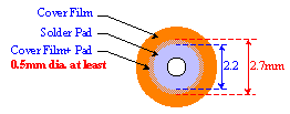
The “Cover Film” must over to the soldering pad to prevent it from peeling off while soldering. |
 |
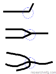
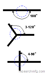
2. Circuit Pattern Guidance
|
Not Recommended |
Recommended |
| No sudden expansion or reduction in pattern width. No sharp angle. | |
|
|
|
|
|
|
3. Design at Folding Area
|
Not Recommended |
Recommended |
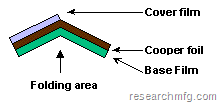
| If the FPC need to be folded then the folding area shall be covered with cover film to prevent trace breaking. | |
|
|
|
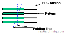
| Avoid folding at below locations to eliminate the possible stress focus a. The change of pattern width. b. Folding parallel to the pattern. |
|
|
|
|
4. Design at Folding Area
|
Not Recommended |
Recommended |
| Plating leads and disconnection holes should be designed as illustrated in order to avoid short circuits. | |
|
|
|
5. Design at Folding Area
|
Not Recommended |
Recommended |
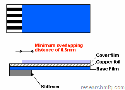
| Avoid ending edge locate at same location for each layer. | |
 |
 |
Related Posts:
- HotBar FPC Design Notices
- Design Guideline for Flex cable(FPC) Trace Pattern
- What potentials cause make HeatSeal Connector peel off?
- Screen-Printing on PET(PolyEthylene Terephthalate) notices
- The Difference Between ED Copper and RA Copper in FPC
- Why RA Copper Is Preferred Over ED Copper for FPC Applications?








Leave a Reply