Working for manufacturer engineering couple years. Sharing the manufacturing experience, skill, DFx, design, and information. Be care of this blog is personal share and content may not be 100% correctly.
The trend in the electronics industry is toward smaller and smaller SMD components, with sizes such as 0402, 0201, and even 01005 becoming common (Note 1). Additionally, the pitch between pins on ICs has decreased to a fine pitch of 0.5mm, and even 0.3mm, posing a challenge for the SMT process.
SMT engineers face the challenge of soldering these thin electronic components onto PCBs without encountering non-wetting or soldering short issues. This task is more difficult when dealing with a mix of larger and smaller parts on a circuit board.
Generally, larger electronic components require more volume of solder on their pins to ensure they are securely attached to the PCB. In contrast, smaller components require less volume of solder, and the amount of solder paste applied must be precisely controlled to avoid the risk of soldering short between pins caused by tiny variations in the amount of solder paste. For example, I/O connectors or power-related components that are exposed to external forces typically require more solder to prevent them from coming loose due to frequent plug and unplug. However, small components are usually designed around or near these bigger size components, some to prevent ESD or voltage surges. Therefore, selecting the appropriate stencil thickness and aperture size becomes a challenging task.
Note 1:
The term “0402” generally refers to the imperial dimensions of electronic passive components for SMD type, which are 0.04″ x 0.02″ (approximately 1.0mm x 0.5mm) in size. Similarly, “0201” represents dimensions of 0.02″ x 0.01″ (approximately 0.6mm x 0.3mm). Other commonly used sizes include 0603, 0805, and 1206.
Not only to deal with various electronic components of different sizes appearing on the same side of a PCB, but we also need to achieve good soldering quality. Therefore, we need to print different thicknesses of solder paste on the same side of the stencil to precisely control the amount volume of solder paste. Thus, a special stencil called “Step Stencil” have been developed.
What is ”Step Stencil” for SMT?
The step stencils of SMT are a type of stencil where the thickness of the steel plate can be partially increased or decreased in certain areas to adjust the amount of solder paste applied, unlike regular stencils where the thickness is uniform throughout. This is achieved by using a thicker steel plate and laser-cutting away the excess material, leaving only the desired stepped areas with varying thickness. For example, a 0.12mm thick steel plate may have stepped areas that are locally increased to 0.15mm, which would be fabricated using a 0.15mm thick steel plate.
What are Step-up stencils and Step-down stencils?
There are two types of step stencils: Step-up stencils and step-down stencils. Step-up stencils are used to partially increase the amount of solder paste applied to certain areas of a PCB, such as for USB or audio jacks, larger components like LGA modules, microswitches, and transformers, or to compensate for coplanarity issues. Step-down stencils are used to reduce the amount of solder paste applied in areas where can effectively control the soldering short problem of FINE PITCH component pins.
As technology advances, it is now possible to use an additional custom-made steel plate that is welded onto the main stencil to create a step-up stencil, but special attention must be paid to ensure that the welded areas are properly smoothed out.
Some limitations for the kind of specific stencils are listed as follows:
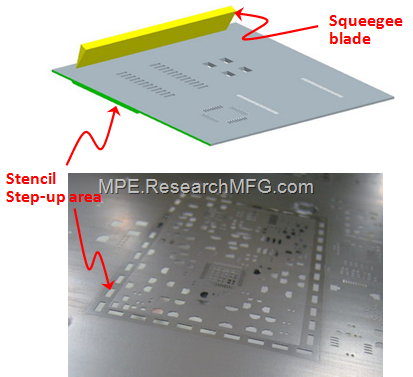
The Left picture shows that the step-up/step-down is processed on the other side of the squeegee blade. It means that the recommended step-up/step-down side should be closed to the PCB to prevent the squeegee blade from being easily damaged. Few step-up/step-down, however, is processed on the same side of the squeegee blade in accordance with some specific considerations.
Of course, this kind of stencils is more expensive than a common stencil since a specific stencil should not only adopt a thicker stencil but also thin the required section by laser. Therefore, a step-down stencil should be easier to manufacture than a step-up one. If there is the requirement of only increasing solder paste volume, it is suggested to increase the aperture size of stencil first to save the cost.
The thickness difference of stencil is recommended within 0.03mm. It means that the thickness of step-up stencil should not be more than 0.18mm if the thickness of the original stencil is 0.15mm. Similarly, the thickness of step-down stencil should not be less than 0.12mm. Although the thickness of stencil can be adjusted based on the requirements, the larger difference of stencil thickness is easier to cause problems in controlling solder paste volume. Since the height of squeegee blade is not easy to be adjusted in accordance with the thickness of stencil during printing, the larger thickness difference of stencil may cause much higher/lower pressure of the squeegee blade, resulting in the excessive/inadequate solder paste volume issue, even distortion problem.
It is better that there is same thickness of step-up/step-down stencil for the area squeegeed by the blade since the blade will prop up at the area. Otherwise, the solder paste volume may be uneven. To avoid the issue, CAD engineers should be requested to design the layout of electronic circuit well. They can arrange the location of parts in accordance with their solder paste volume requirements. In fact, most of step-up stencils will thicken partial area instead of the whole area. Therefore, it should be more careful to print solder paste with these stencils.
In the edges of step-up/step-down on a stencil, 3~5mm space should be reserved at least in order to mount other small parts requiring less solder paste volume, or larger ones requiring more solder paste volume. Since the squeegee blade may not fit the variation of stencil thickness in time, the solder paste may not be printed into the aperture well. Therefore, the space of edge is designed to avoid the insufficient solder paste volume issue.
When operating the kind of step-up/step-down stencils, the speed of squeegee blade should be slower to ensure good transfer efficiency of solder paste. Also, the downward pressure of the squeegee blade should be controlled well.

 The trend in the electronics industry is toward smaller and smaller SMD components, with sizes such as 0402, 0201, and even 01005 becoming common (Note 1). Additionally, the pitch between pins on ICs has decreased to a fine pitch of 0.5mm, and even 0.3mm, posing a challenge for the SMT process.

及下鋼板(Step-down stencil)階梯鋼板?")


Leave a Reply