A user asked: “How is the thickness of the stencil determined? What considerations are there for the shape of the stencil apertures?”
The thickness of the stencil is mainly determined by the amount of solder paste needed for component soldering. Thinner stencils usually mean less solder paste deposited during printing. The amount of solder paste required for each solder joint depends on the components on the printed circuit board (PCB), especially those sensitive to solder volume, such as BGAs with the smallest ball pitch and fine-pitch components. Additionally, smaller components demand higher precision in solder paste printed. Ultimately, the decision also depends on the quality of solder joints after soldering.
Factors determining stencil thickness, aperture and shape
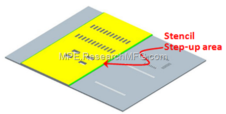
When determining stencil thickness, priority is given to the solder volume required for these fine-pitch components mentioned earlier. For example, for 0402 components, a stencil thickness of 0.12mm is commonly used, while 0201 components typically require a 0.10mm thickness. As components become smaller and the number of fine-pitch components increases on the same side of PCB, some may opt for a 0.08mm stencil thickness. Additionally, for components requiring more solder paste, stepped stencils, which locally increase thickness, are used. However, there are limitations to the thickness of these stepped areas, typically allowing an increase of 0.01 to 0.08mm. Moreover, the presence of nearby fine-pitch components near the stepped area must be considered. The sudden elevation caused by the step during squeegee action may lead to local deformation. If there are apertures near the edge of the stepped area, uneven solder paste deposition or excessive solder paste may occur.

In addition, thinner stencils result in less stable control over solder paste printed on the PCB. This means that the precision of solder paste printed on the PCB decreases because the vertical surfaces of stencil apertures are not as smooth as imagined. Depending on different stencil manufacturing processes such as etching, laser cutting, coating, and electroforming, different surface roughness may occur. The rougher the surface of the apertures, the more likely solder paste residue will remain on the vertical surfaces. Once this happens, it leads to insufficient solder paste deposition in subsequent printing. Factors like squeegee pressure, speed, angle, and solder paste type (solder powder particle size) also affect the quality of solder paste printing.
Size and shape of stencil apertures
Regarding the size and shape of stencil apertures, they are generally based on a 1:1 ratio with the pad size and shape on the PCB. Then, modifications may be made to the aperture size and shape for some special components to meet their soldering requirements. Some components may require the use of stepped stencils to locally increase or decrease the amount of solder paste.
It is recommended to refer to the IPC-7525 Stencil Design Guidelines document. This document stipulates:
-
To ensure that solder paste can be perfectly transferred through the stencil apertures onto the printed circuit board, the document requires that a certain ratio between the aperture size and thickness of the stencil be maintained to prevent solder paste from being unable to deposit due to surface tension.

-
Aspect Ration = Width of Aperture / Thickness of Stencil Foil = W/T > 1.5
pitch (mm) 1.27
0.80
0.55
0.40
pad width (mm) 0.635
0.40
0.275
0.20
stencil thickness (mm) <
(W/T >1.5)0.42
0.27
0.18
0.13
- Area of Aperture Opening / Area of Aperture Walls = (LxW) / [2x(L+W)xT] > 0.66
-
-
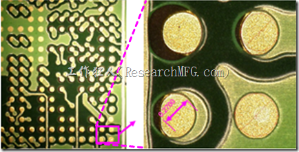
For PBGA packaged components: It is recommended to reduce the solder paste printed diameter by 0.05mm compared to the pad size to avoid short circuits.
-
For CBGA packaged components: It is recommended to expand the diameter by 0.05mm to 0.08mm compared to pad size to prevent solder skip. This is because there is a significant difference in the coefficient of thermal expansion (CTE) between ceramics and FR4, resulting in a large difference in thermal deformation.
-
For fine-pitch BGA and CSP packaged components: If the aperture is square, it is recommended to reduce each side by 0.025mm and round off the four corners. When the side length is 0.25mm, the rounding radius should be 0.06mm, and when the side length is 0.35mm, the rounding radius should be 0.09mm to facilitate soldering and prevent short circuits.
-
Recommendations for chip components such as resistors, capacitors, and inductors:
Generally, small chip components are prone to solder bead issues during SMT soldering. Besides solder paste oxidation, the main reason for solder beads is the rapid evaporation of flux contained in the solder paste at high temperatures, carrying some of the solder paste outward (think of it as a “popcorn” effect). As a result, separated solder paste blocks are formed in the small gaps between the component body and the PCB. During reflow, since there are no solder pads under the component to absorb the molten solder and with the weight of the component body, the separated molten solder will emerge from under the component and form small solder beads at its edges.
Therefore, small chip components typically use two types of aperture shapes, namely the inverse home-plate and home-plate shapes, to reduce the amount of solder paste printed, allowing the flux to evaporate smoothly to prevent solder bead formation and short circuits. As for the aperture size, it is generally recommended to use 1/3 of the pad width (W) or length (L), but it is strongly recommended to adjust the size appropriately according to the characteristics of your own product.
If you’re concerned that reducing the amount of solder paste might affect solderability, like solder skip, you can consider using half-moon or round-shaped solder paste printing apertures to reduce the amount of solder paste. However, round apertures may increase the problem of solder paste residue on the sidewalls of the stencil apertures, causing unstable solder deposition. Therefore, it’s advisable to conduct experiments before using round apertures.
For components with tombstone issues, you can consider using the home-plate shape and slightly expanding it towards the tip of the home-plate, or slightly offsetting the entire solder paste aperture towards the tip of the home-plate to resolve the issue. However, this is just a temporary solution. It’s best to address tombstoning issues through PCB design by increasing thermal relief and reducing the inner pad dimensions to solve the problem permanently.
-
For components like MELF cylindrical parts: It is recommended to use a C-shaped aperture to avoid the issue of component displacement due to rolling.

Related Posts:


Leave a Reply