Since the electronic product design moves from desktop to portable devices, the manufacturer also make electronic component as small as possible to meet this popular trend. Besides, the PCB thickness also become thinner and the associated soldering pads on the PCB are tiny size. This make the SMT manufacturing process more difficult and challenge.
You may know that portable device always has BGA malfunction risk during impact drop test. Most of company dispense the underfill glue to fix this kind of BGA crack issue. My company did the same thing too. WorkingBear think there shall be another way to enhance the soldering pad strength to eliminate the underfill glue since underfill process spend money and waste labor hours.


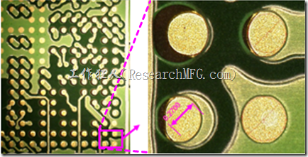
There are two kinds of BGA land patterns design. One is Copper Defined pads design and also called as NSMD (Non-Solder Mask Defined) pads design. Refer to above picture show the solder mask open size is bigger than the copper pad size.
The benefits for NSMD pads design are:
-
Good solderability. The soldering area is not only the copper pad surface but also the surrounding side of copper pad.
-
PCB supplier will be easily control the soldering pad size and the location of the NSMD. Because of the copper pad is registered by optical exposure skill and it is more accurate technology.
-
Besides, the trace layout will be more easily as compare to another design since copper pad size is small.
The disadvantages for NSMD are:
-
NSMD pads design is easily peeled off from outside stress. Because of small pad size results in small pad bonded strength on the PCB. For example, BGA ball crack during impact drop test.
-
Many of the company apply the underfill glue to enhance the BGA bonding strength. The underfill process make the manufacturing cost up and waste the material and labor. The underfill also makes the repair difficult since glue is fixed under the BGA.
 |
Another pad design is called SMD (Solder Mask Defined), also known as Copper Defined pad. |
The benefits for SMD pads design are:
-
SMD pads design has better copper pad bonding strength on PCB. It also improve the BGA bonding strength. Because of the copper pad size of SMD is bigger than the NSMD. More copper size the more PCB bonding strength.
-
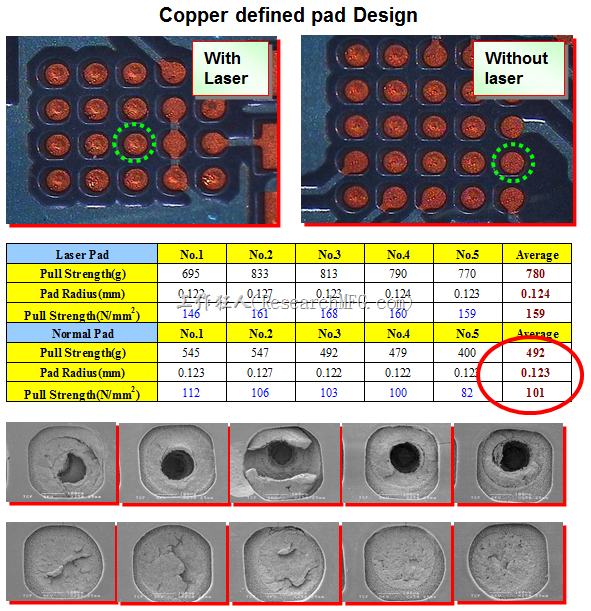
SMD pads design has better performance to be survived from the impact drop test. According to the data provided from PCB supplier show there are 53% improvement of the pad bonded on PCB strength as compare between SMD and NSMD pads design.
(Please note that this experimental test data does not involve solder balls. It is purely testing the strength of the solder pads through pull testing. If you want to evaluate the ability of BGA solder balls to withstand stress after soldering, it is necessary to perform pull tests on the solder balls after they have been soldered. You shall not be misled by this data.)

The disadvantages for SMD are:
-
The SMD pads design will lower the soldering strength. Because of the solder mask will be expanded its dimension and reduce the soldering size during reflow high temperature stage.
-
The solder mask printing will shift due to poor tolerance control. This will make position discrepancy between the BGA ball and pad on PCB. Some serious case will affect to solder pad dimension on PCB.
-
The trace layout is more difficult between pads for SMD pads design. Because the bigger pad size make the small space between pads.
WorkingBear still strongly encourage implementing the SMD pads design. Because of SMD pads design had enhanced the BGA strength. It is really high potential to remove the underfill process.
(Please note that WorkingBear’s suggestion regarding whether to use SMD or NSMD design for BGA solder pads should depend on individual products. There is no definitive answer as to which type of solder pad design is best. WorkingBear’s blog has multiple articles discussing solder cracking topic, and it is recommended to review all of these articles instead of making a decision based on a single article.)
Below pictures show the pad bonded force on PCB of SMD pad design is better than NSMD pad by about (155-101)/101=53% improvement.
(Please note that this experimental test data does not involve solder balls. It is purely testing the strength of the solder pads through pull testing. If you want to evaluate the ability of BGA solder balls to withstand stress after soldering, it is necessary to perform pull tests on the solder balls after they have been soldered. You shall not be misled by this data.)


- With laser: Indicates the BGA solder pad has a laser-drilled via.
- Without laser: Indicates the BGA solder pad does not have a laser-drilled via.
BGA solder pads with laser-drilled vias have better resistance to pulling forces than those without, but the vias must be electroplated and plugged, or else insufficient solder may occur during SMT process, causing voids or solder paste covering the vias, leading to blowhole issues.
Related Articles:


Leave a Reply