This article will talk about the composition of the PCBA bonding-force.
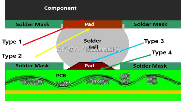
There are numerous factors and elements involved in PCBA bonding force. However, Workingbear believes that we can utilize the findings of the red dye test to examine this issue. The Red Dye Penetration test of BGA have categorized cracks into five types of defect locations. These positions can also be applied to all soldering problems in PCBA.
Type 1. The bonding-force between Cu Pad (Copper foil) on the component and component substrate
The copper foil bonded to the BGA substrate is represented. If different types of electronic components are used, the bonding force will differ due to variations in substrate material, plating, and bonding solutions on the soldering terminals.
Type 2. The bonding-force between BGA ball and Cu pad on component
The IMC layer at the component site is represented.
The BGA package typically employs a Nickel (Ni) substrate base, resulting in an IMC of Ni3Sn4. It shall be noted that components with dissimilar plating material on the soldering terminals will yield distinct IMC compositions, leading to varying bonding-force.
Type 3. The bonding-force between BGA sphere/ball and Cu pad (Copper foil) on the PCB
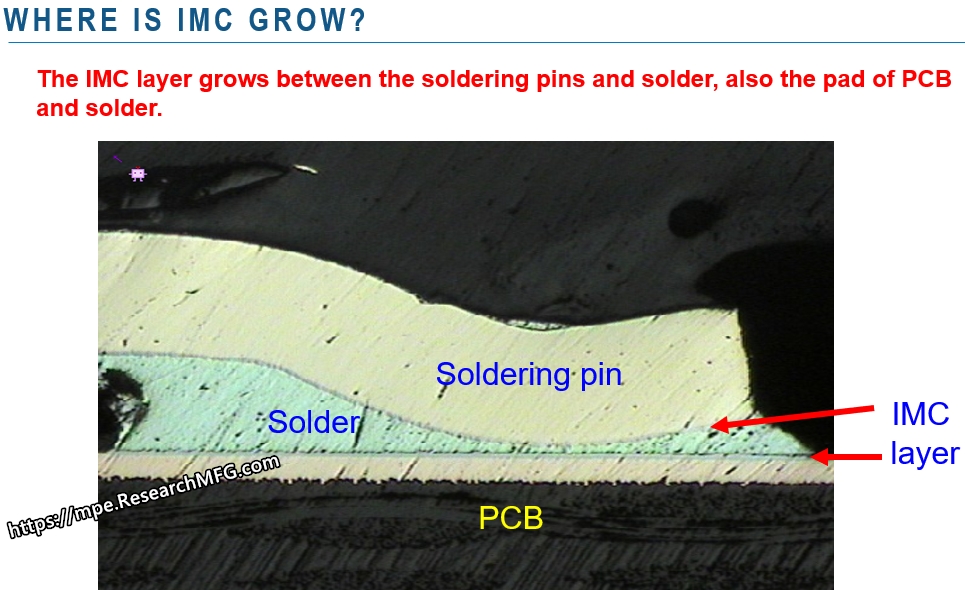
The IMC layer grows during SMT is represented.
Different PCB surface finishes can lead to distinct types of IMC and result in varying bonding forces. The Cu base of the PCB will generate an IMC of Cu6Sn5, the Ni base of the PCB will produce an IMC of Ni3Sn4. In general, the bonding-force of Cu6Sn5 is superior to that of Ni3Sn4. Unfortunately, over time, the Cu6Sn5 will gradually transform into a weaker bonding-force of IMC of Cu3Sn.
Type 4. The bonding-force between Cu pad (Copper foil) on PCB and PCB laminate (FR4)
The copper foil bonded on the PCB substrate (FR4) layer is represented.
To enhance the copper foil pad on FR4, it is recommend to use NSMD (Non-Solder-Mask-Defined) pad design. Nevertheless, NSMD is unsuitable for BGA ball solderability, which we can discuss in subsequent article.
Sometimes, humidity can trigger PCB delamination problems since moisture expands rapidly during high-temperature in reflow process.
Type 5. The bonding-force within solder ball
Voids inside the solder ball is represented.
For the other components then the solder paste quality and voids is the key.
By now, you should already be aware of the various bonding forces present in a PCBA. The next step is to identify the weakest point, as cracks tend to begin at this point when stress is applied.
Experience has shown that over 60% of solder cracks occur in the IMC layer located on the PCB side. (Do you remember what IMC stands for?) The second most common site of failure is between the copper foil pads on the PCB and the FR4, while the third is between the IMC layer of the BGA ball and the Cu pad on the component side. Only a few of the cracks occur within the solder ball or solder itself.
When people analyze solder cracks in BGAs or components and find a slightly black color on the broken section, they often assume that oxidation on the component or PCB soldering surface is the root cause of the crack. Does this true? We found the color of IMC layer is generally fainter than the fresh-solder since it been exposed at atmosphere quite a long time and most of the solder crack just happen at IMC layer. Therefore, checking the color of the crack section may not provide accurate information.
Still have question? In the previous article, it was stated that the IMC layer is a necessary condition for good solder formation. So why do solder cracks always occur at the IMC layer?
Article series :
- Why BGA soldering ball always crack(1)? Stress > bonding-force
- Why BGA soldering ball always crack(3)? IMC layer growth is a certain result to form the soldering joints
- Why BGA soldering ball always crack(4)? Using “copper” base material as the surface finish for PCB
- Why BGA soldering ball always crack(5)? Increase the contact area of solder to increase its strength
- Why BGA soldering ball always crack(6)? The recommendation of BGA pad design from Workingbear
- Why BGA soldering ball always crack(7)? The Bonding force between solder pad of copper foil and PCB substrate
- Why BGA soldering ball always crack(8)? Increase PCB stiffness to resist stress and avoid board bending
- Why BGA soldering ball always crack(9)? Increase the resistance of components to stress
- Why BGA soldering ball always crack(10)? Reduce the impact of PCB bending through the mechanism design change
- Why BGA soldering ball always crack(11)? Stress is the Biggest Culprit in Causing BGA Solder Joint Cracks
- Why BGA soldering ball always crack(12)? Manufacturing Processes That May Generate Significant Stress
- Why BGA soldering ball always crack(13)? Usage Environment is the Biggest Challenge of Stress Sources
Related article:
Increase solder paste volume will improve the MLCC capacitor broken?


I have a question concerning BGA ball crack. A phenomenon was observed, after a product was deployed in the field and few months later reported functional failure. Analysis led to BGA and eventually cross-section show that the corner tip BGA ball cracked. But it was cracked at the component FR4 side, not the product PCBA side of it. The customer assumed it was related to strain/strain rate but a thorough checked in our processes had proven all the data was below the IPC-9704 defined (least square )straight line. By design, there is a need to use a tool to push the locking pin to secure the heatsink at 2 corners. But the strain/strain rate was good. So, I can’t help but to think the BGA IMC layer might have a problem. Customer internally had another opinion was on the nickel thickness. My question is, what is the role play of the nickel, and reading your article, you suggest IMC should be between 1 to 5 um but I understood this is a by-experience numbers. Is there other factors I need to consider what could cause the BGA ball crack at the component side? (totally cracked away from component FR4).
Stephen Lim,
If you read my article about the “Waht is IMC?” then you will find “The IMC layer can be grown and distributed evenly at the interface location will be good enough.“. So you need to check IMC layer of BGA grows evenly and not focus on the thickness of the IMC layer.
The IMC will be Ni3Sn if your PCB is ENIG finished. That means the Nickel will be one element of IMC instead of the copper in OSP finished.
Back to your BGA ball crack issue, as I said “the crack is because stress > bonding force”. I do recommend you check the strain/stress by gage at each stage may give the stress to the PCBA include testing, assembly process and drop testing.