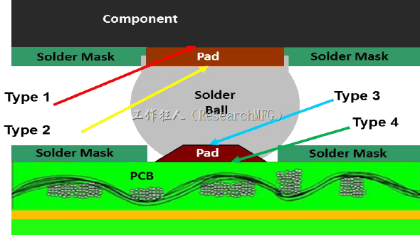
Following last discussion, we learned that solder cracking is caused when the stress placed upon it exceeds the strength of the bonding force. However, it’s possible to address this issue by increasing the bonding force of the printed circuit board assembly (PCBA). By doing so, we can effectively eliminate solder cracking, making it a more reliable and robust technology for a wide range of applications.
So, Is that any solution to enhance the bonding force for PCBA?
Of course, if you’re looking to enhance the bonding force of your printed circuit board assembly (PCBA), there are several solutions available to you. For example, many R&Ds prefer asking manufacturer to increase the solderability or select the enhancement FR4 material (higher Tg) to increase the bending resistance. However, the effectiveness of these solutions will depend on the amount of money you’re willing to spend. Here are a few aspects to consider and potential solutions for increasing the bonding force.
The following several articles will explain the advantages, disadvantages, and precautions of several methods to increase the bonding force of PCA:
I. Using “Copper” Base Material as the Surface Finish for PCB
Different PCB surface finished combined with solder paste will produce various IMC soldering compounds, which will lead to different solder joint strength. Because of the major material of solder paste is tin. Currently, the PCB surface finish used in the industry can be basically divided into two types: “copper” and “nickel”.
ENIG (Electroless Nickel Immersion Gold) is the representative of the “nickel” base PCB surface finish. After soldering, “nickel” will combine with “tin” to form Ni3Sn4 IMC intermetallic compound. OSP (Organic Solderability Preservatives), HASL (Hot Air Solder Leveling), Im-Sn (Immersion Tin), and Im-Ag (Immersion Sliver) are all “copper” base PCB, and after soldering, they will combine with “tin” to form Cu6Sn5 IMC.
Basically, the bonding force of Cu6Sn5 is stronger than Ni3Sn4. Overall, the strength of the IMC formed by the “copper” base PCB and the solder paste is basically stronger than that of the nickel base. Therefore, using a “copper” base process for PCB surface finish can increase solder joint strength. However, the IMC of the “copper” base will gradually aged into the inferior IMC Cu3Sn after a period of time, and its solder joint strength will become relatively brittle and weak, but this may take several years to occur.
In addition, all IMC layers will gradually thicken over time, and high temperature will accelerate the growth rate of IMC layer. As mentioned before, the strength will decrease after the IMC becomes thicker, but this is also a problem that may occur several years later. Only those who require a long service life and military specifications need to pay special attention to the problem of IMC transformation and thickening.
In fact, there is also a Immersion silver board (Im-Ag) on the market, which is also a copper base PCB surface finish. People applied it when the lead-free process was first phased in, but there were too many quality problems. It also requires special attention to avoid “sulfur” and “sulfide” pollution, and now only few boards still use it, so we will not discussed it here.
ENIG surface finish PCB also have a potential risk, which is the problem of “black nickel” or call “black pad”. If it occurs, it will seriously affect the quality of soldering. For details, please refer to the article “Two potential problems of ENIG surface-treated PCB solder pads (black nickel and rich phosphorus layer) and preventive measures”.
Therefore, if your company happens to use ENIG surface-treated PCB, you can consider changing the surface finish to OSP (Organic Solderability Preservatives) or HASL (Hot Air Solder Leveling) or Im-Sn (Immersion Tin)! However, different surface treated (finished) PCB have different shelf life, and some surface-treated PCBs even strictly require to reduce the time for the board to pass through the first and second reflow ovens. The soldering effect may also be different on the first and second sides of the board, and the usage conditions for entering the reflow oven after the PCB is opened also vary. Pay special attention when choosing. For details, please refer to the article “Advantages and disadvantages of several common PCB surface finish”.
Article series :
- Why BGA soldering ball always crack(1)? Stress > bonding-force
- Why BGA soldering ball always crack(2)? The composition of PCBA bonding-force
- Why BGA soldering ball always crack(3)? IMC layer growth is a certain result to form the soldering joints
- Why BGA soldering ball always crack(5)? Increase the contact area of solder to increase its strength
- Why BGA soldering ball always crack(6)? The recommendation of BGA pad design from Workingbear
- Why BGA soldering ball always crack(7)? The Bonding force between solder pad of copper foil and PCB substrate
- Why BGA soldering ball always crack(8)? Increase PCB stiffness to resist stress and avoid board bending
- Why BGA soldering ball always crack(9)? Increase the resistance of components to stress
- Why BGA soldering ball always crack(10)? Reduce the impact of PCB bending through the mechanism design change
- Why BGA soldering ball always crack(11)? Stress is the Biggest Culprit in Causing BGA Solder Joint Cracks
- Why BGA soldering ball always crack(12)? Manufacturing Processes That May Generate Significant Stress
- Why BGA soldering ball always crack(13)? Usage Environment is the Biggest Challenge of Stress Sources
Related article:
Increase solder paste volume will improve the MLCC capacitor broken?


Leave a Reply