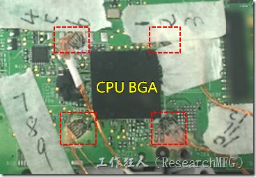
Below are recommendations for BGA pad design to enhance the soldering strength from Workingbear.
We had several pages talking about the relationship between solder cracking and bonding force. Workingbear personally doesn’t think that making design a change to the pad of PCB can help much with the ability of BGA soldering to resist stress, as it is like a drop in the bucket! A board’s bending or deformation can easily negate all your efforts in improving pad design and solderability. Workingbear still thinks that strengthening the mechanism design and improving the board’s ability to resist bending and deformation is the best solution to fix BGA solder cracking.
However, as a process engineer, WorkingBear must come up with the best BGA pad design solutions for R&D to refer to, so as not to be seen as someone who only talks about work without actually contributing, and to avoid being criticized for shirking responsibility and leaving everything to others. Below is the recommendation for BGA pad designs from :
-
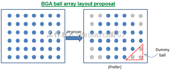
Design SMD pads on the outermost row of the BGA’s balls. If possible, design the outer two rows of balls in the four corners of the BGA as SMD pads. However, SMD pads will reduce the space for signal routing.
-
Design other pads as NSMD pads to provide more space for signal routing.

-
SMD pads will enhance the bonding force of the pads, which can solve the problem of pads being pulled up, but it is not good for the soldering of the balls themselves. Therefore, if solder cracking still occurs between the BGA balls and pads with the above SMD pad design, Workingbear will suggest changing the outermost row of the BGA’s ball pad back to NSMD pad, and adding via holes and electroplating and plugged. This is because the bonding force between NSMD pads and FR4 is not good enough, and adding via holes is like adding rivets to the pads, which can enhance their bonding force with FR4. However, this will increase the cost of the PCB by about 10%.
-
Please notice no best pad design can completely solve the problem of BGA solder ball cracking. You shall take responsibility for your product by experimental design to get a better pad design solution. Again, using solder to resist the impact stress is not a good solution.
Article series :
- Why BGA soldering ball always crack(1)? Stress > bonding-force
- Why BGA soldering ball always crack(2)? The composition of PCBA bonding-force
- Why BGA soldering ball always crack(3)? IMC layer growth is a certain result to form the soldering joints
- Why BGA soldering ball always crack(4)? Using “copper” base material as the surface finish for PCB
- Why BGA soldering ball always crack(7)? The Bonding force between solder pad of copper foil and PCB substrate
- Why BGA soldering ball always crack(8)? Increase PCB stiffness to resist stress and avoid board bending
- Why BGA soldering ball always crack(9)? Increase the resistance of components to stress
- Why BGA soldering ball always crack(10)? Reduce the impact of PCB bending through the mechanism design change
- Why BGA soldering ball always crack(11)? Stress is the Biggest Culprit in Causing BGA Solder Joint Cracks
- Why BGA soldering ball always crack(12)? Manufacturing Processes That May Generate Significant Stress
- Why BGA soldering ball always crack(13)? Usage Environment is the Biggest Challenge of Stress Sources
Related article:
Increase solder paste volume will improve the MLCC capacitor broken?


Leave a Reply