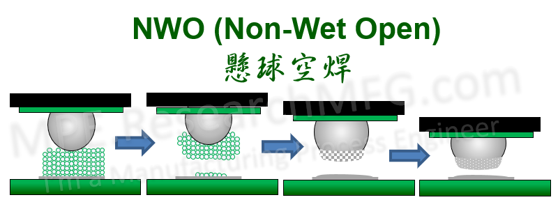
Recently, many have inquired about how to deal with Non-Wet-Open (NWO) issues when encountering BGA packaged ICs soldering. The defects associated with NWO are quite similar to those of HIP (Head-in-Pillow) and typically occur at the edges and corners of BGA packaged ICs. The root cause often lies in the substrate or PCB of the BGA, where the board material may deform due to the high temperatures during the reflow process.
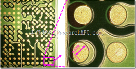
The visual appearance of NWO defects is strikingly similar to HIP or call HoP (Head-on-Pillow) issues. NWO defects present as a solder ball seemingly loosely attached to the PCB soldering pad, often appearing as a single ball or with tiny, almost imperceptible balls on the pad. In contrast, HIP manifests as a solder ball partially resting on another solder, usually exhibiting a dual-ball phenomenon.
There are various possible causes for NWO, including board deformation, oxidation of solder pads/pads, insufficient temperature for tin melting, misalignment in solder mask printing, and more. However, more than 80% of the issues often stem from board deformation.

Observing the defects caused by NWO, it’s conceivable that X-ray inspection might reveal the issue. Since the solder paste printed on the soldering pad is almost entirely absorbed by the BGA solder balls after reflow for NWO, it’s reasonable to assume that the diameter of the solder balls at the NWO location might be larger than other normal solder balls. Under the condition that the pad size and volume of solder paste printing for each solder ball are the same, there’s a chance to detect this with a conventional 2D X-ray inspection. However, caution is advised, as an inexperienced observer might not easily identify the problem. It’s recommended to consult with an experienced engineer for a thorough inspection.
Causes of NWO defect: Board Deformation
During the continuous heating and soaking in the reflow oven’s soak zone, the PCB undergoes gradual bending and deformation due to the elevated temperatures. Typically, PCBs use board materials with a glass transition temperature (Tg) around 150°C to save costs. As the temperature inside the reflow oven increases, PCB deformation becomes more pronounced, reaching temperatures as high as 250°C for SAC reflow. Additionally, thinner board thickness and heavier component loads can exacerbate deformation due to gravitational forces.
Some of the solder paste originally applied to the PCB pads might stick to the solder balls of the BGA. As the temperature rises inside the reflow oven, the gap between the BGA’s solder balls and the PCB increases. The solder paste gradually moves towards the BGA’s solder balls, eventually adhering completely to them. When the furnace temperature reaches the melting point of the tin alloy, the gap between the BGA’s solder balls and the PCB pads is maximized. In other words, when the solder balls and solder paste fully melt, they do not make contact with the PCB pads until the reflow oven’s temperature returns and below the solder melting point.
As the reflow oven begins to cool below the solder melting point, the PCB gradually returns to its original shape from the bent deformation (although in some cases, it may not fully recover). However, by this point, all the solder paste adhering to the BGA’s solder balls has already merged with the solder balls. Upon cooling, when it makes contact with the pads, it merely rests loosely on the PCB pads without a true solder joint. If the PCBA undergoes slight deformation again due to certain conditions, an open circuit may occur, leading to the observed Non-Wet-Open (NWO) phenomenon on the PCB pads.
Solution: Minimizing Board Deformation
Regardless of whether you’re dealing with HIP or NWO, the solutions primarily involve reducing the occurrence of board bending and increasing the amount of solder paste on BGA soldering pads (more accurately, increasing the height of the solder paste printed). Although there are strategies in place, they may not guarantee a 100% solution, and the investment might not always justify the returns. Therefore, it’s essential to evaluate and decide on the most effective approach to minimize the defect rates.
Further Reading:
- Causes and Prevention Methods for Board Bending and Warping
- Can Increasing Solder Paste Improve BGA Soldering?
- How to Solve the HIP (Head-In-Pillow) Defect in BGA Solder Balls
Cause of NWO defect: Oxidation of Solder Pads
As explained earlier, NWO defect is essentially the phenomenon where solder paste fails to adhere to the solder pads on PCB. If oxidation occurs on the solder pads, it can lead to the Non-Wet-Open issue too, even if the PCB does not deform due to high temperatures.
Solution: Address PCB Issues for Oxidized Solder Pads
If the cause is oxidized solder pads, the solution lies in addressing the issues with the PCB. If the PCB surface finish is ENIG, pay attention to the thickness of the immersion gold. Thinner gold thickness (less than 1.0µ”) may lead to oxidization issues. If the surface finish is OSP, run the second reflow as soon as possible after the first reflow is completed.
Another aspect related to PCB surface treatment is HASL. If the tin spraying thickness is insufficient, there might be difficulty achieving proper wetting during the second reflow, as a substantial amount of tin may have already formed intermetallic compounds (IMC) with the underlying copper during the initial reflow.
Cause of NWO defect: Insufficient Temperature on Solder Pads
Another factor contributing to NWO is the inability of solder pads to reach the required temperature for effective solder melting. This issue commonly arises in the central solder ball region of BGAs or in solder pads connected to large copper foils and covered by solder mask or inner layer.
Central Solder Ball Region of BGAs: Particularly in large BGA packages with numerous solder balls in the middle, the heating of the pads underneath is impeded by the package itself. The heating progression starts from the outermost pads and moves inward. If the reflow temperature profile is not well-adjusted, it may lead to insufficient heating in the central region, causing NWO or HIP. This often occurs in RTS reflow temperature profiles.
Solder Pads Connected to Large Copper Foils: Solder pads connected to extensive ground copper foils can slow down the rate of temperature rise. Most of the heat is absorbed by the copper foil, and when other pads have reached the required temperature, these pads connected to large copper foils may not have reached the necessary temperature. As a result, the solder paste on these pads can be taken away by solder balls with higher temperatures on the BGA. Once the reflow oven temperature starts to drop, NWO may occur.
Solution: Optimize Reflow Oven Temperature Profile
A common recommendation is to adjust the reflow oven temperature profile to achieve optimization, which is a cost-effective method. Consider increasing the soak zone time to ensure that all solder pads reach a certain temperature before entering the reflow zone.
Additionally, for solder pads connected to large copper foils, it is advisable to modify the layout by introducing a design with thermal relief pads to effectively reduce the chances of most heat being absorbed by the extensive copper foil.
Further Reading:
RSS or RTS? Which SMT Profile Should You Choose?
SMT Reflow Soldering Temperature Profiles Explanation and Precautions
Related Posts:
- The Hidden Dangers of Using Overdue PCBs: Can Baking Salvage Them?
- What Process Impact of Substituting SMDs with Paste-In-Hole components?
- Preventing BGA Solder Joint Cracking: Strengthening Design from the Source
- Differences, advantages, disadvantages, and recommendations for SMD and NSMD pad designs


Leave a Reply