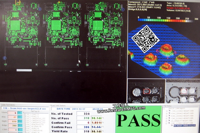
AOI (Auto Optical Inspection) is an automated optical recognition system that has become widely used in the electronics industry for inspecting the quality of soldering, component placement accuracy and the presence of missing components on PCBA (Printed Circuit Board Assembly) production lines, replacing human visual inspection processes.
(Please note: The AOI mentioned in this article refers to 2D AOI. Nowadays, there are 3D AOIs available on the market that provide more detailed three-dimensional image inspection, improving the detection rate of AOI.)
The basic principle of AOI technology is to use imaging techniques to compare the tested and stored object with standard images to determine if there are significant differences, thereby judging whether the testing object meets the standards. Therefore, the effectiveness of AOI largely depends on its image resolution, imaging capability, and image analysis technology.
In its early stages, AOI was mainly used to detect defects in surface markings after encapsulation of ICs (integrated circuits). With technological advancements, it is now employed on SMT assembly lines to inspect the quality of solder joints on PCBA or to verify if solder paste printing meets standards through SPI (Solder Paste Inspection).
The benefit of implementing AOI in SMT lines:
The primary advantage of AOI is its ability to replace human manual visual inspection both before and after SMT reflow, offering a more precise detection of PCB assembly defects compared to human inspection. However, similar to human visual inspection, AOI is limited to cosmetic inspections of visible features. Consequently, it can accurately inspect shapes and features that are visible on the surface. However, it may overlook solder joints concealed under components or located at the edges of tall components. Many AOIs now incorporate multi-angle photography to enhance their capability to detect IC lead lifting and to capture additional views of obscured components, thereby improving detection rates. Nevertheless, achieving a 100% test coverage rate remains challenging due to the occasional limitations in effectiveness.
The drawback of AOI
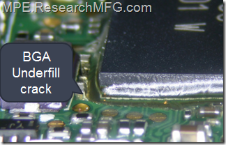
Actually, AOI also has a major drawback in that it’s prone to false rejects in areas where grayscale or shadow contrast is not very clear. These areas could possibly be distinguished using different colored lights, but the most troublesome scenarios involve components covered by other parts and solder joints beneath components. Traditional AOI can only detect areas reached by direct light, meaning components hidden under shielding frames or at their edges might be missed by AOI.
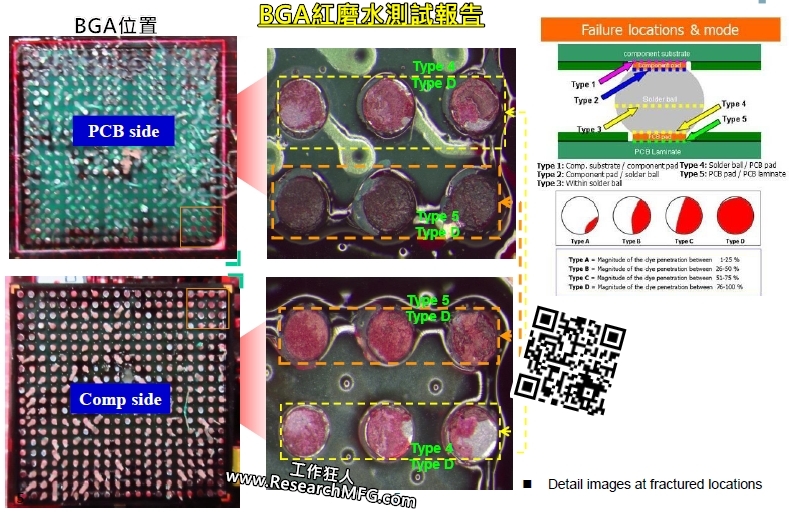
So, in general, PCB assembly production lines rarely rely solely on AOI to ensure PCB assembly quality. Typically, they also undergo ICT (In-Circuit Test) and functional verification testing (FVT). Some lines even include an additional AXI (Automatic X-ray Inspection) station, which uses X-rays to inspect the quality of solder joints (like BGA) beneath components, ensuring a 100% test coverage rate for the PCB.
Youtube: AOI (Auto Optical Inspection)-TRI7100
What defects can AOI detect in assembled PCBs?
Based on Workingbear’s understanding, current AOI systems should be able to fully detect the following PCB assembly defects, most of which can also be identified through huma manual visual inspection without errors:
- Missing components

- Skewed components

- Tombstoning

Additionally, due to optical inspection being limited by factors like lighting color, angles, and resolution, the following defects may only be detectable under certain conditions, making it challenging to achieve a 100% detection rate:
-
Wrong components: Different-shaped or differently marking on components top surface can usually be detected, but those with no obvious differences in appearance, like resistors and capacitors smaller than 0402 size without marking on it, are difficult for AOI to detect.
-
Wrong polarity: This depends on whether the component itself is marked with polarity symbols or has differences in appearance.
If there are no cosmetic differences, then AOI cannot defect component polarity. -
Lead lifting and deformation: Severe lead lifting can be identified by differences in light reflection, but mild cases may be challenging. Severe lead deformation are easily detected by AOI, while detecting mild lead deformation depends on various factors and the experience of engineers or operators.


-
Solder bridges (short): Solder bridges (short) are generally easy to detect, but those hidden beneath components are challenging. For example, solder bridges in connectors often occur at the bottom of the component body, making them undetectable by AOI.

-
Insufficient solder: Significant solder shortages are easily identified by AOI, but variations in solder paste printing may introduce errors, necessitating the collection of a sufficient number of products for assessment.

-
Non-wetting, de-wetting and cold soldering: These are particularly troublesome issues because they are difficult to detect visually. Even if their appearance can be used for judgment, the differences are minimal, and overly strict parameter settings may lead to misjudgments. Calibration over time is often needed to optimize the parameters for such issues.
In summary, although AOI is useful, it does have inherent limitations. However, it can be used for real-time initial analysis of SMT quality and immediate feedback to improve SMT processes, effectively increasing SMT yield.
Typically, using ICT, MDA and FVT equipment to detect problems and then informing SMT for correction often involves a time lag of more than 24 hours. By then, the status of SMT has usually changed, and even the production line may have switched. From a quality control perspective, AOI indeed serves a necessary purpose.
Furthermore, with the advancement of 3D technology and improved MCU (Micro-Controller Unit) processing capabilities, many equipment manufacturers are now developing 3D AOI technology. In addition to achieving differentiation, the 3D AOI’s imaging technology is more realistic than traditional 2D images, making it easier to identify problem areas.
Related Posts:


Leave a Reply