

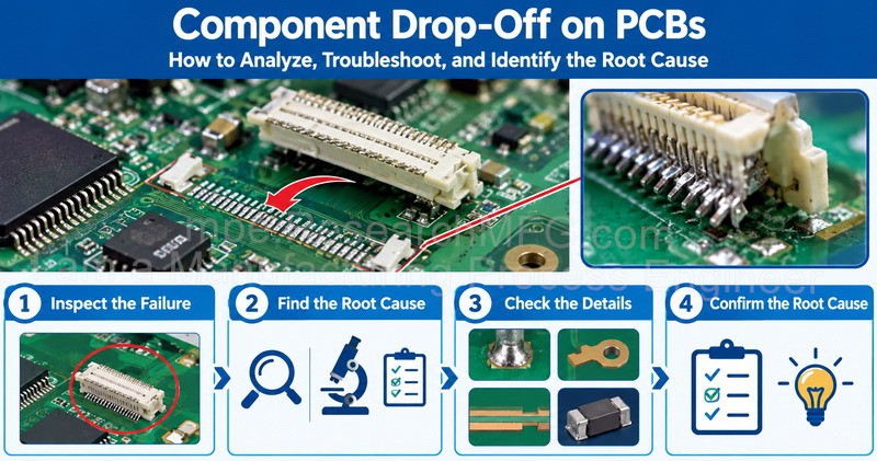
Components falling off a PCB can be a nightmare for many process and quality engineers. Workingbear has previously shared several cases involving components falling off PCBs. However, the root cause can be different in every case. Many engineers, especially those who are new to this type of failure, may not know where to start when they encounter a component detachment problem. So, I would like to share the approach and analysis steps I typically use as a practical reference.
(Of course, I welcome other professionals to share their own experience and insights. Different opinions and discussions are how we learn and improve. Workingbear does not claim that this is the best or only way to analyze the problem. It is simply a summary of my own practical experience.)

In general, when a component falls off a PCB, the problem is usually related to either soldering quality or design-related issues. In many cases, the root cause can be traced to one or more of the following conditions, either individually or in combination:
- There is a problem with the PCB surface finish.
- There is a problem with the component lead or terminal finish.
- Poor storage conditions caused the PCB or component to oxidize.
- There is a problem with the reflow soldering temperature profile.
- The assembled PCBA was exposed to excessive PCB bending or external impact during a subsequent manufacturing process.
- The solder joint was not strong enough to withstand the mechanical stress encountered during actual use.
7 Steps for Analyzing PCB Component Drop-Off Failures:
The following is the general procedure I use to analyze component drop-off failures. Some of these activities could technically be combined into the same step, while others are closely related to the next step. So if anything is unclear, feel free to leave a comment and discuss it.
Step 1: Gather Information
This step is very important. If the information at the beginning is wrong, all the effort and analysis that follows may be wasted.
First, confirm the exact failure description with the person who reported the problem. Then try to collect as much of the following information as possible:
- What exactly happened? Try to describe the failure as clearly as possible. Under what circumstances did the component or product fall off? Was the product dropped? What kind of environment was it used in, such as a gas station, outdoors, or indoors? Was air conditioning available? Was the product exposed to any special environmental conditions or tests, such as high- or low-temperature testing?
- Did the problem occur at the customer’s site or during the manufacturing process? At which step in the manufacturing process was the problem first observed or discovered?
- When did the problem occur? Was it discovered during production, or only during final product testing? Are the failures concentrated within the same date code?
- What type of surface finish does the PCB use? ENIG? OSP? HASL? ENIG can have black pad issues, HASL can have solderability problems after the second trip through the reflow process, and OSP can develop solderability problems when the material is past its shelf life.
- What is the PCB thickness? 0.8 mm? 1.0 mm? 1.2 mm? 1.6 mm? The thinner the PCB, the more likely it is to warp or bend, which can also increase the possibility of solder cracking.
- What type of finish is used on the component leads or terminals? Matte tin? Gold plating?
- What is the main alloy in the solder paste? SAC305 (tin-silver-copper)? SCN (tin-copper-nickel)? SnBi (tin-bismuth low-temperature solder paste)? Different solder alloys have different melting points.
- If possible, it is best to retrieve the reflow temperature profile recorded at the time of production.
Recommended reading: What Is the 5W1H Method? A Practical Guide to Clear Thinking and Better Communication
Step 2: Obtain the Failed Unit and Preserve the Evidence for Further Analysis
Whenever possible, obtain the actual failed PCB. If the component has completely fallen off, it is best to recover the loose component as well. This gives you both sides of the failure for comparison and allows for a more complete analysis. If more than one failed unit is available, obtain as many samples as practical based on the situation.
Step 3: Check the PCB’s Solderability
After obtaining the failed sample, check the solderability of both the PCB and the component terminals, and compare the differences between them.
When checking solderability, it is recommended to inspect the solder joints under a microscope. This makes it much easier to identify subtle problems that may not be visible to the naked eye.
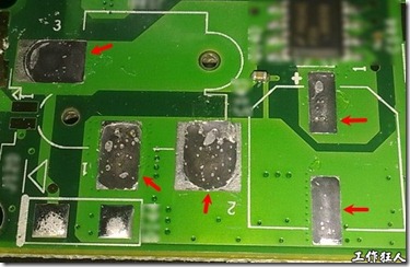
Check the solder on the PCB pads for defects such as non-wetting or de-wetting. These problems are usually related to poor PCB surface finish or improper PCB storage conditions, which can cause the pads to oxidize and result in poor solderability.
Of course, there are also cases where the solder simply cannot wet the pad because the reflow temperature was too low. In this situation, you can use a soldering iron to check whether the pad can accept solder. If the pad cannot be wetted even with a soldering iron, the problem can almost certainly be traced back to the PCB itself.
Please note that some HASL PCBs use a tin-copper-nickel (SCN) alloy, which has a melting point about 10°C higher than SAC305. SAC305 has a melting point of approximately 217°C, while SCN melts at approximately 227°C.
If you can further rule out oxidation caused by improper PCB storage conditions, you can ask the PCB supplier to inspect the product directly or return the PCB to the supplier for further analysis.
If there is still a dispute, you can first measure the thickness of the surface finish. For ENIG, the thickness of both the gold and nickel layers should normally be checked. For HASL, check the thickness of the solder coating. For OSP, check directly for signs of oxidation.
If the cause is still unclear, a cross-section should be performed for a more detailed analysis.
Recommended reading:
Step 4: Check the Solderability of the Fallen Component’s Terminals
It is also recommended to inspect the solderability of the component terminals under a microscope. This makes it easier to identify subtle conditions that cannot be seen with the naked eye.
Check whether the component terminals were properly wetted by solder. It is also a good idea to examine the composition of the plating on the component terminals and determine whether its melting or dissolution behavior is compatible with the reflow temperature. Some components use a sputtered silver (Ag) coating. Because the sputtered silver is only deposited on the component surface, the silver can be readily dissolved into SAC solder during reflow, potentially reducing the solder joint strength.
Please note that some component terminals may have exposed copper on their cut surfaces where no plating is present. These areas generally do not solder well, but they are normally designed to be located in areas where solder wetting is not required or is not critical. For example, the side terminations of a QFN do not necessarily need to be wetted with solder.


Step 5: Check Whether the Component Took the PCB Pad with It When It Fell Off

If the solderability of both the PCB pads and the component terminals appears to be normal, check whether the PCB pads have been peeled off from the board or remain attached to the fallen component terminals. If the pads have been pulled away from the PCB, this is also evidence that the solder joint between the component and PCB was strong. It provides further evidence that the reflow process itself was not necessarily the problem.
If the PCB pad did not come off with the component, first check whether the reflow temperature profile met the solder paste manufacturer’s requirements. If additional failed samples are available, it is also a good idea to use a soldering iron to see whether the component can be soldered back onto the PCB. If the component can be successfully soldered back in place, it may indicate that the process window can be improved by adjusting the reflow temperature or solder paste. However, a component push test is recommended.
Take a known-good PCB and compare its push strength with a PCB produced using the newly adjusted solder paste and reflow profile. If there is a difference in push strength, the PCB surface finish should be investigated further. In some cases, a poor surface finish can cause localized pad oxidation. ENIG may have a black pad issue, while the second reflow pass of a HASL PCB can sometimes result in excessive IMC formation.
Recommended reading:
Step 6: Examine the Fracture Surface Where the Component Fell Off
Use a microscope to inspect the fracture surfaces on both the PCB pads and the component terminals. Under proper lighting, check whether the fracture surface is rough or smooth. A rough fracture surface usually indicates that a one-time external force caused the component to be pulled off. A smooth fracture surface is more commonly associated with failure caused by long-term vibration or a weak solder joint.
If the PCB uses ENIG, another possibility is black pad, which can cause the solder joint to separate along the nickel layer.
Step 7: Cross-Section Analysis and EDX Elemental Analysis of the IMC

If none of the previous steps can clearly identify the cause of the component drop-off, the final step is to perform a destructive cross-section analysis. When doing this, it is recommended to cross-section both the PCB and the fallen component.
There are two main purposes for the cross-section analysis:
- Check whether IMC (Intermetallic Compound) has formed and whether the IMC layer is uniform. IMC formation is an important indicator of solder joint quality. EDX should also be used to verify the composition and elemental ratios of the IMC to determine whether they are normal. The exact IMC thickness is not necessarily the most important factor. However, if the IMC grows unevenly or is missing in certain areas, the solder joint strength can be reduced, resulting in lower component push strength. Poor IMC growth can be caused by oxidation or insufficient temperature during soldering.
Determine which layer the fracture occurred in.
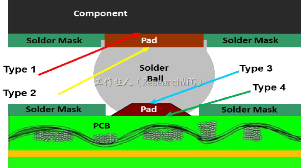
If the fracture occurs within the IMC layer, it usually indicates that solderability was not the primary problem. Instead, the solder joint may simply not have been strong enough to withstand the external mechanical force. This is generally a design issue that needs to be addressed. However, some R&D engineers may choose to add underfill or adhesive to BGA or other components to provide additional mechanical reinforcement.If the fracture does not occur within the IMC layer but instead occurs on the PCB side, the problem is more likely to be related to the PCB.
Conversely, if the fracture occurs on the component side, the problem is more likely to be related to the component.
Recommended reading:
The above is simply a summary and sharing of my personal experience. I welcome you to share your own methods for analyzing and troubleshooting component drop-off failures.
Related Posts:
- BGA Failure Analysis: Manufacturing Issue or Design Flaw?
- Solution to Prevent Component Drops During Second Time Reflow Soldering
- How to Evaluate the Risk and Probability of Electronic Components Not Falling Off during SMT Second Reflow
- Why Don’t devices Fall Off on First Side during SMT Second Reflow? Does the solder MP increase during the second reflow?



Leave a Reply