Working for manufacturer engineering couple years. Sharing the manufacturing experience, skill, DFx, design, and information. Be care of this blog is personal share and content may not be 100% correctly.
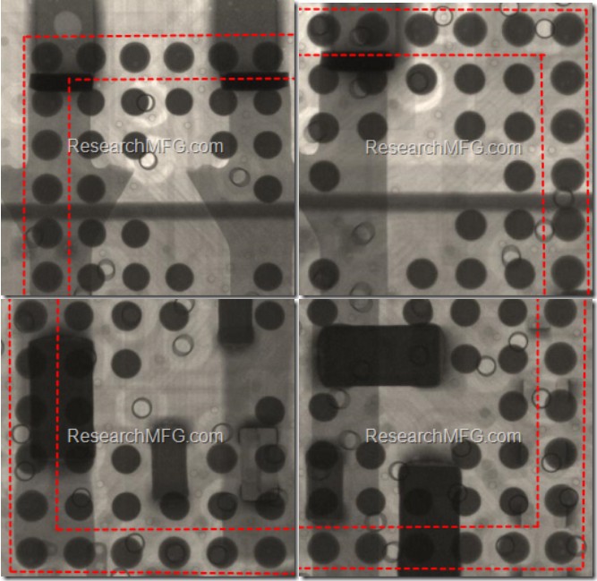
X-ray image of a BGA showing more solder on the outer rows than on the inner rows.
Improving BGA solder joint quality is an ongoing goal for SMT engineers, especially when working with fine-pitch BGA components. In general, BGAs with a ball pitch of 0.8 mm or less are considered fine-pitch devices, although the exact definition may vary slightly among manufacturers.
BGA soldering is challenging because all the solder joints are located underneath the component body. After reflow, it is difficult to inspect the solder joints visually or with AOI (Automated Optical Inspection) equipment. In some cases, even X-ray inspection cannot reliably determine whether a BGA has open or false solder joints. Certain X-ray systems with oblique-angle imaging or 5DX technology may be able to detect some BGA soldering defects. However, these systems are expensive, and their cost may make them impractical for routine, in-line inspection in high-volume production.
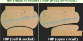
In our experience, one of the most common BGA soldering defects is HIP (Head-in-Pillow), also known as HOP (Head-on-Pillow) or double-ball effect. This defect can occur when the PCB passes through the high-temperature zones of the reflow process, following the reflow temperature profile. The heat can cause both the PCB substrate and the BGA package to warp. When the solder paste and BGA solder balls melt, the warpage can cause them to separate, preventing them from making proper contact. As the temperature drops below the solder’s melting point, the PCB and BGA package gradually return toward their original shapes. However, by that time, the solder paste and solder balls may already have solidified. This can leave two distinct solder surfaces stacked together without forming a reliable metallurgical joint. This is the well-known HIP defect.
Figure caption: Head-in-Pillow defect show on the outermost roww of BGA solder balls.
More than 90% of HIP defects are typically found along the outermost rows of BGA solder balls, especially at the four corners. This is because the diagonal distance across a BGA package is the longest, making the corners particularly susceptible to warpage. The outermost rows are generally the next most vulnerable areas.
Based on these observations and experiments conducted by experienced SMT engineers, increasing the solder volume can effectively reduce HIP defects caused by thermally induced warpage of the PCB and BGA package. However, increasing the solder paste volume too much can create solder bridging and short circuits, so the amount must be carefully controlled.
For this reason, Workingbear recommends selectively increasing the solder paste volume on the outer rows of BGA pads rather than increasing it at every pad. You might wonder whether this increase could raise the risk of insufficient soldering or open joints. The key point is that we achieve this by modifying the size and shape of the stencil apertures, rather than changing the stencil thickness using a step-up or step-down stencil. This approach helps ensure that the solder paste remains in contact with all BGA solder balls after component placement, minimizing the risk of open joints. The additional solder paste provides extra volume to accommodate warpage of the BGA substrate and PCB during reflow.
One way to adjust the solder paste volume is to modify the stencil apertures. The basic principle is to deposit more solder paste on the outermost rows or corner solder balls than on the inner solder balls, without adding too much. This helps maintain sufficient contact between the solder paste and the BGA solder balls even when the PCB and package warp at high temperatures.
When the BGA solder ball diameter is greater than 0.4 mm:
Increase the solder paste volume along all four outer rows of BGA solder balls. Change the stencil apertures from circular openings to square openings that circumscribe the original circular pads. Keep the apertures for the remaining inner pads circular and maintain their original solder paste volume. This approach increases the solder paste volume on the outermost rows by approximately 27.4% compared with the inner pads.
When the BGA solder ball diameter is less than 0.4 mm:
Keep the circular stencil apertures and solder paste volume unchanged for the outermost rows. For the inner solder balls, reduce the solder paste volume by changing the stencil apertures to smaller square openings that fit inside the original circular pads. With this approach, the solder paste volume on the inner pads is approximately 36.3% lower than that on the outermost rows.
With either approach, the solder paste volume on the outermost rows will be approximately 27–36% greater than that on the inner solder balls. The goal is to maintain sufficient solder paste contact with the BGA solder balls while the PCB and package deform at reflow temperatures.
The X-ray image below shows a BGA with solder balls smaller than 0.4 mm, where the solder paste volume on the inner rows was reduced. If you look closely, the solder deposits on the outermost rows appear slightly larger than those on the inner rows. In other words, the dark circular areas representing the solder deposits have slightly larger diameters along the outer perimeter.
Figure caption: X-ray image of a BGA with solder balls smaller than 0.4 mm, showing reduced solder paste volume on the inner rows. The dark circular areas representing the solder deposits are slightly larger along the outermost rows.Figure caption: Picture shows the actual stencil aperture result for BGA package with ball sizes less than 0.4mm in diameter
Precautions
When modifying a stencil, verify that the stencil thickness and aperture dimensions meet the area ratio requirements specified in IPC-7525.
When the solder ball pitch is 7 mil or greater and the stencil thickness is less than 4 mil, pay particular attention to the risk of solder bridging and short circuits.
Final Note
If the problem you are trying to solve is voiding inside BGA solder balls, increasing the solder paste volume may not resolve it.





Leave a Reply