


Do you know the difference between SMD (Solder Mask Defined) and NSMD (Non-Solder Mask Defined) pad designs for PCB? What are the advantages and disadvantages of each? More importantly, which pad design provides better resistance to BGA solder joint cracking under mechanical stress?
A few years ago, our company went through a management change. It’s a familiar story in many companies—new managers often like to introduce new ideas to make their presence felt. One of the first changes was a new PCB design rule: all future BGA layouts should use NSMD pads instead of SMD pads. The idea was that NSMD pads would create stronger solder joints, making BGAs more resistant to mechanical stress and increasing the likelihood of passing impact drop tests and tumble tests.
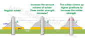
The reasoning seemed straightforward. With the same exposed copper area, an NSMD pad allows solder to wet both the top surface and the sidewalls of the copper pad, while an SMD pad allows solder to wet only the top surface because the solder mask overlaps the edge of the pad. In theory, this gives NSMD pads a larger solder joint and better resistance to board flex and impact.
From the standpoint of solder joint strength alone, the theory makes sense. If both pad designs have the same exposed copper area, an NSMD pad generally provides a larger solderable surface because solder can wet both the top surface and the sidewalls of the copper pad. As a result, the solder joint itself is typically stronger than one made with an SMD pad.
However, does that necessarily mean an NSMD pad design makes a BGA more resistant to drop-related failures in real-world applications? Not necessarily.
To find out, we once conducted an experiment using two versions of the same PCB—one with SMD pads and the other with NSMD pads under the BGA. We then performed pull tests on the entire BGA package. The results were quite different from what the new manager expected. However, they also didn’t prove very much, because neither design was able to pass the product qualification (DQ) drop test or tumble test.
In fact, our results were inconsistent. Sometimes the NSMD design performed slightly better, while other times the SMD design came out ahead. We simply couldn’t prove that one design was consistently superior to the other. If you’ve had different experiences, I’d love to hear about them.
Later, we realized that pulling on an entire BGA package introduces many variables that can influence the results. In another project, following Workingbear’s suggestion, we tested only the individual solder balls using shear and pull tests. Once again, neither SMD nor NSMD showed a clear advantage.
Later, we realized that pulling on an entire BGA package introduces many variables that can influence the results. In another project, following Workingbear’s suggestion, we tested only the individual solder balls using shear and pull tests. Once again, neither SMD nor NSMD showed a clear advantage.
What these results tell us is that improving solder joint strength alone is unlikely to solve BGA solder cracking problems. If the real issue is excessive mechanical stress caused by PCB flexing or product design, increasing solder strength by itself may not produce the results you’re hoping for.
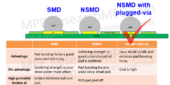
The following table summarizes the advantages and disadvantages of SMD and NSMD pad designs. The comparison assumes that both pad types have the same exposed copper area.
| SMD (Solder-Mask-Defined) |
NSMD (Non-Solder Mask Defined) |
|
|---|---|---|
 |
 |
|
| Advantages | Stronger bonding between the copper pad and the FR-4 substrate because the actual copper pad is larger. | Larger solderable area and stronger solder joints because solder wets both the top surface and the sidewalls of the pad. Easier PCB routing because there is more space to route traces between adjacent pads. |
| Disadvantages | Smaller solderable area results in slightly weaker solder joints. The solder mask overlapping the pad edge may also affect solder wetting because of differences in thermal expansion. PCB routing is more difficult. |
Weaker pad-to-FR-4 bonding because the copper pad itself is smaller. Flux residue and solder balls are more likely to remain around the exposed copper outside the solder mask opening. |
| Most Likely Failure Location | Between the solder ball and the PCB pad, typically at the IMC (Intermetallic Compound) layer. | Between the copper pad and the FR-4 substrate, where the pad may peel away from the PCB. |
To date, there is no conclusive evidence showing that either SMD or NSMD is universally superior for preventing BGA solder joint failures caused by mechanical stress. In Workingbear’s view, the best long-term solution is to address the root cause of the stress through better PCB and product design, rather than relying solely on stronger solder joints.
That said, if PCB manufacturing cost is not a major concern, Workingbear generally recommends using NSMD pads with plugged copper-filled vias-in-pad whenever practical. Properly filled vias help eliminate soldering issues associated with open vias, and the pad size should be maximized whenever the PCB layout permits. Based on our testing, pads with copper-filled vias consistently demonstrated higher shear and pull strength than pads without vias.

If you’re interested in learning more about BGA solder joint cracking and component detachment, be sure to check out Workingbear’s related article series on this topic:
If you’ve had different experiences or opinions, feel free to leave a comment and join the discussion!
Related Posts:
- Underfill Techniques for Enhanced BGA and CSP Assembly
- Red Dye Penetration Test to check for BGA solder joint cracking
- Concept Clarification: IMC Layer Fracture Despite the Formation of Effective Solder Joints
- What is ENIG Surface Finished for Circuit Boards? What Are Its Advantages and Disadvantages?
- What is IMC (Intermetallic Compound)? How does IMC relate to PCB solder joint strength? Are there IPC standards for IMC thickness?





Leave a Reply