

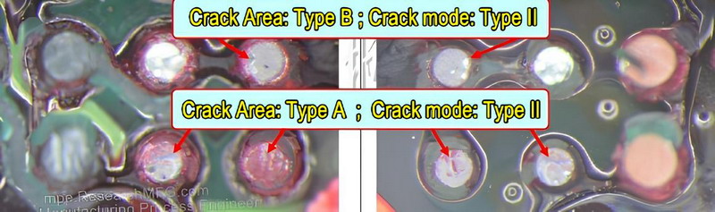
When a BGA fails and the Red Dye Penetration Test reveals cracked solder balls, how can we determine the actual root cause? Does the Red Dye Penetration Test simply tell us that a solder ball is cracked, or can we use the results to identify why the crack occurred?
BGA solder ball cracking can generally be associated with several failure mechanisms, including HIP (Head-In-Pillow), HoP (Head-On-Pillow), NWO (Non-Wet-Open), and mechanical stress applied after soldering. In many cases, more than one factor may contribute to the failure.
The most reliable way to determine the actual failure mechanism is to perform a cross-section and examine the fracture surface under a scanning electron microscope (SEM). This provides more direct and objective evidence for identifying the root cause. However, before performing a cross-section, electrical testing should first be used to identify which solder balls are associated with the failure. This allows us to target the suspected solder balls for cross-sectional analysis.
Recommended reading:
- Red Dye Penetration Test to check for BGA solder joint cracking
- BGA Red Dye Penetration Test: Acceptance Criteria for Cracks and Voids
To be honest, I personally do not recommend using the Red Dye Test as the first choice for analyzing BGA solder ball cracking. The test can easily introduce errors, and even a small mistake during the procedure can alter or destroy the original failure evidence. It can also be difficult to determine the true root cause, and the test cannot reliably tell us whether the fracture occurred within the IMC (Intermetallic Compound) layer.
That said, the Red Dye Test is still one of the most affordable ways to check for BGA solder ball cracks. If you have an oven and the appropriate red dye, the test can even be performed in-house. However, keep in mind that it is a destructive test. If you only have one failure sample, I recommend using X-ray inspection to check for solder opens first. A fiber-optic camera can also be used to inspect the solder balls along the outer edges of the BGA for possible HIP or NWO defects.
If you have enough failure samples rather than just one, Workingbear would recommend using the Red Dye Test as a preliminary verification before performing a cross-section. In most cases, the Red Dye Test can tell us whether the solder balls are cracked and show how the cracks are distributed across the BGA.
Strictly speaking, after the Red Dye Test, the fracture surfaces should be examined under a high-magnification microscope. We need to determine whether the fracture surface is smooth and rounded or rough. This information can then help us determine whether the failure is more likely to be related to an SMT process issue such as HIP/HoP or NWO, or to mechanical damage caused by assembly or by the product being dropped during use.
So, when performing a Red Dye Test, the following observations should be recorded:
-
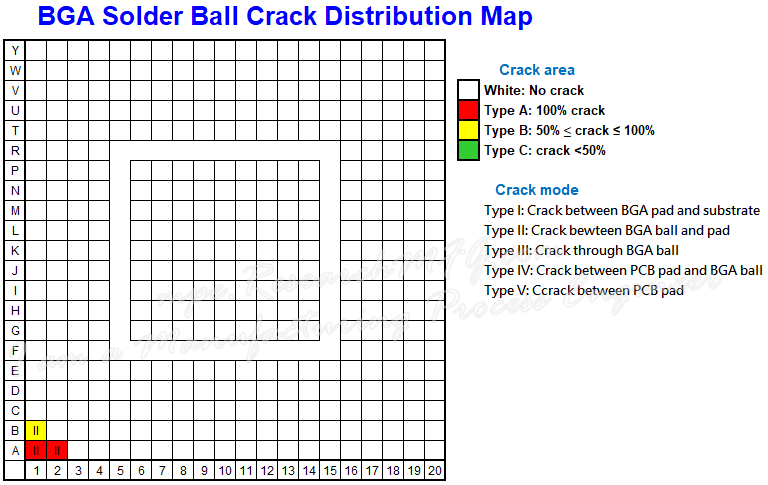
Record the percentage of each solder ball area that has been stained by the red dye penepention.
-
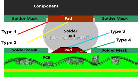
Observe and record where each solder ball has fractured: between the solder ball and the BGA substrate, between the solder ball and the PCB, or through the middle of the solder ball.
If the fracture occurs between the solder ball and the BGA substrate, check whether the BGA pad has delaminated and whether the red dye has penetrated into the delaminated area.
If the fracture occurs between the solder ball and the PCB, perform the same checks on the PCB pad.
If the crack occurs through the middle of the solder ball, examine the shape of the fracture surface. -
Record the appearance of every fracture surface, including whether it is smooth or rough.
How to Interpret the Red Dye Test Results (Multiple Failure Mechanisms May Be Involved):
-
If the fracture occurs between the solder ball and the BGA substrate, continue by checking whether the BGA pad has delaminated and whether the red dye has penetrated into the delaminated area. If so, the failure may be related to BGA substrate quality or insufficient pad adhesion strength to withstand external mechanical stress. This information can also help determine whether the responsibility lies with the BGA substrate supplier.
-
If the fracture occurs between the solder ball and the PCB, check whether the PCB pad has delaminated and whether the red dye has penetrated into the delaminated area. If there is no pad delamination, the failure may be related to an NWO soldering issue. However, the fracture shape and surface roughness should also be examined. If the PCB pad has delaminated and the red dye has penetrated into the delaminated area, the failure may be related to PCB manufacturing quality or insufficient pad strength to withstand external mechanical stress.
-
If the fracture occurs through the middle of the BGA solder ball, examine whether the fracture surface is rounded, smooth, rough, or relatively flat. A smooth, rounded fracture surface may indicate HIP, while a rougher or less uniform fracture surface is more likely to be associated with external mechanical stress.
If the failure is related to NWO or HIP, it is more likely to be an SMT process issue. These defects are often caused by warpage of the PCB or BGA substrate during the high-temperature reflow process. The amount of warpage is also affected by the product design. For example, an uneven copper distribution or copper traces that are too thin on the PCB can make the board more susceptible to warpage. Another possible factor is oxidation of the solderable surface or solder coating.
Recommended reading: Causes and Prevention of PCB Warping and Bending After Reflow
Common Misinterpretations When Using the Red Dye Test:
- Do not jump to the conclusion that red dye penetration is an SMT process defect.
When red dye penetrates into a solder joint during the Red Dye Test, it only tells us that the solder ball is cracked. It does not tell us why the crack occurred or whether it was caused by the SMT process. We still need to examine the fracture surface. A smooth, rounded fracture surface may indicate HIP/NWO, while a rough fracture surface is more likely to be associated with external mechanical stress. Without this additional analysis, it is easy to misidentify the root cause and blame the wrong process or supplier. - Always confirm the fracture location and check whether the pad has delaminated.
Simply looking at whether the solder ball has been stained red ink is not enough. You need to determine whether the crack occurred on the component side, PCB side, or through the middle of the solder ball, and whether the pad has delaminated. Otherwise, insufficient pad adhesion or a PCB lamination problem could easily be mistaken for a simple solder ball crack. - Do not rush to perform a Red Dye Test when only one sample is available, and do not treat the result as the final root cause.
The Red Dye Test is destructive. When samples are limited, X-ray and fiber-optic inspection should be performed first. Even after a Red Dye Test has been performed, accurate root-cause identification may still require cross-sectioning and SEM/EDX analysis to avoid drawing an incomplete conclusion.
BGA solder ball cracking caused by external mechanical stress can generally occur under the following conditions:
- Board-level testing
Board-level testing often uses test fixtures such as bed-of-nails testers. If the mechanical stress is unevenly distributed across the fixture, it can cause BGA solder ball cracking. A strain gauge or strain measurement system can be used to identify the location and magnitude of the stress. - Final product assembly
Poorly designed product assembly processes can cause the PCB to bend. Possible causes include screw fastening, locating clips, or mechanical supports in the product housing that are not on the same plane. These conditions can also be evaluated using a strain measurement system. - Impact from a product being accidentally dropped by the customer
A product dropped during use can generate significant PCB bending and mechanical stress. A strain measurement system can be used to simulate the deformation and stress generated during a drop event. - Thermal expansion and contraction caused by changes in environmental temperature
This cause is relatively uncommon because it should normally be identified during the product development stage through environmental simulation and testing. However, it can still occur if the appropriate environmental tests were not thoroughly performed.
Please note that when solder ball cracking is caused by mechanical stress, the crack will naturally tend to start at the weakest point of the structure. If the solder joint was not properly formed during the SMT reflow process, the fracture would typically occur between the BGA solder ball and the PCB pad, assuming material oxidation is not a factor. If the PCB pad is too small to withstand the mechanical load from vibration, drops, or long-term PCB bending, the pad itself may be pulled away from the PCB. However, this type of pad delamination can also be caused by poor PCB lamination during PCB manufacturing.
Recommended reading: BGA Solder Ball Crack Analysis Using the Red Dye Test | Types and Failure Patterns
Related Posts:
- Why BGA soldering ball always crack(1)? Stress > bonding-force
- Improve BGA Solderability By Partially Increasing Solder Paste Volume
- Preventing BGA Solder Joint Cracking: Strengthening Design from the Source
- Preventing Solder Cracks in BGA Designs: Strengthening Tips from the Design End
- [Case Study] BGA Solder Ball Cracking: Strain Gauge Analysis and Design Improvement
- Should BGA Pads Be Designed as SMD or NSMD? Pros, Cons, and Drop-Test Performance



Leave a Reply