

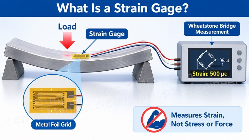
A strain gage (also spelled strain gauge) is a thin, resistive sensor that is bonded to the surface of an object to measure mechanical deformation. When the material is stretched, compressed, bent, or twisted, the metal foil grid inside the strain gage deforms along with it, causing a change in electrical resistance. A Wheatstone bridge circuit converts this very small resistance change into a measurable voltage signal, which can then be used to calculate the strain.
One important point to understand is that a strain gage directly measures strain, not stress or force. Stress and force must be calculated indirectly from the measured strain using the material’s mechanical properties, such as Young’s modulus, or determined through calibration.
The operating principle can be expressed using the Gage Factor (GF):
\[ GF = \frac{\Delta R / R}{\varepsilon} \]
Where:
-
\(\Delta R\): Change in electrical resistance caused by strain
-
\(R\): Electrical resistance before deformation
-
\(\varepsilon\): Strain
For conventional metal foil strain gages, the gage factor is typically around 2. This means that a strain of 500 µε applied to a 350 Ω strain gage produces a resistance change of only about 0.1% (= 2 × 0.0005), or approximately 0.35 Ω.
Such a small resistance change is difficult to measure accurately with an ordinary digital multimeter. Even if a reading can be obtained, the measurement error may be significant. For accurate results, a Wheatstone bridge circuit and a precision strain measurement instrument or signal conditioner should be used.
In practical applications, strain is commonly expressed in microstrain (µε), where 1 µε represents a relative deformation of one millionth. When a metal conductor is stretched, its length increases and its cross-sectional area decreases, causing its electrical resistance to increase. Compression produces the opposite effect.
Common Applications of Strain Gages
The basic function of a strain gage is to convert mechanical deformation into an electrical signal. Therefore, strain gages are useful whenever we need to determine whether a structure is deforming excessively, whether it is experiencing abnormal loading, or whether it can withstand repeated loading over its intended service life. Common applications include:
-
Experimental stress analysis: Strain gages are bonded to mechanical structures, brackets, enclosures, and fixtures to verify whether actual strain measurements agree with FEA (Finite Element Analysis) simulations and to identify areas of stress concentration.
-
Force, weight, and pressure measurement: Load cells, pressure sensors, and torque sensors commonly use strain gages as their sensing elements. They are widely used in electronic scales, automated equipment, weight inspection systems, and force feedback applications.
-
Fatigue and reliability testing: Repeated loads are applied to structural components while strain data is recorded over time. The results help evaluate the risk of cracking, yielding, permanent deformation, and fatigue failure.
-
Torsion and rotating shaft measurement: Strain gages can be bonded to shafts or rotating components and combined with slip rings or wireless data transmission systems to measure torque and power.
-
Residual stress analysis: A common method uses a three-element rosette strain gage bonded to the material surface. A small hole is then drilled to release the residual stress, and the resulting strain changes are used to calculate the original residual stress.
Applications of Strain Gages in the Electronics Industry
For electronics manufacturers and PCBA (Printed Circuit Board Assembly) factories, strain gages are particularly useful for understanding how mechanical deformation is transferred from the enclosure or mechanical structure to the PCB, connectors, shielding cans, and solder joints. They help verify whether mechanical deformation is excessive enough to damage electronic components or cause solder joint cracking.
| Application | What Can Be Measured |
|---|---|
| PCB bending tests | Local strain caused by screw fastening, connector insertion and removal, or heatsink installation |
| BGA / CSP solder joint reliability | Whether PCB strain near the package exceeds allowable limits during thermal cycling, drop tests, or board bending |
| Connector insertion and removal | PCB deformation and solder joint strain caused by the insertion force of high-pin-count connectors, and whether the strain is excessive enough to damage solder joints or pads |
| Shielding can / metal component fastening | Local strain and stress concentrations caused by installation, riveting, or screw fastening |
| Enclosure and bracket validation | Whether excessive mechanical strain is transferred to the PCB during drop, vibration, or torsion tests |
| Fixtures and production equipment | Deformation and long-term fatigue of SMT, press-fit, and test fixtures |
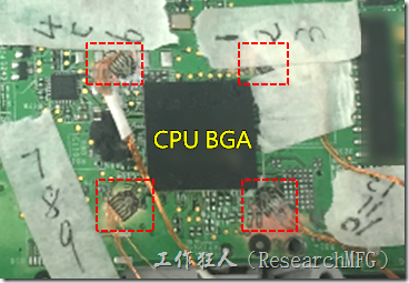
One of the most common applications is measuring PCB strain around BGAs and other large packages. In practice, strain gages are often bonded to the backside of the PCB near the four corners of a BGA. Strain is then measured in real time during operations such as screw fastening, connector insertion and removal, heatsink installation, or drop testing.
The measured strain values are compared with the allowable strain limits provided by the component manufacturer to determine whether the mechanical loading could cause solder joint cracking, pad cratering, or package damage. This type of measurement helps identify assembly-related mechanical stress that cannot be directly detected through visual inspection or X-ray inspection.
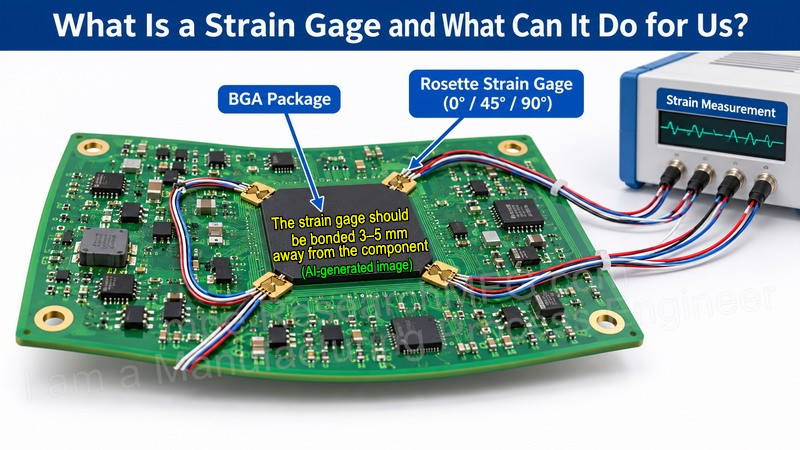
When installing strain gages, choose the side of the PCB with sufficient available space. Since the component side is often occupied by BGA packages and other components, the backside of the PCB is usually the preferred location. If there is not enough room on the backside either, the strain gages may need to be installed on the component side. In some cases, nearby small components may have to be removed to provide enough space for installation.
If the principal strain direction at the measurement location is unknown, a three-element rosette strain gage can be used. A common configuration is the 0°/45°/90° rosette. By measuring strain in multiple directions simultaneously, the magnitude and direction of the principal strains can be calculated.
It is important to understand that a strain gage primarily measures in-plane strain (tensile, compressive, and shear strain) on the PCB surface. It does not directly measure out-of-plane displacement in the Z direction. However, when a PCB bends, the in-plane strain on its top and bottom surfaces will have opposite signs. If the strain gage is bonded to the convex side of the bent PCB, the surface is stretched and the measured strain will be positive. If it is bonded to the concave side, the surface is compressed and the measured strain will be negative.
Therefore, the strain difference between the top and bottom surfaces can be used to indirectly calculate the bending curvature and out-of-plane PCB deformation (warpage).
Types of Strain Gages
Strain gages can be classified in several different ways. The most common classifications are described below.
1. Classification by Sensing Element Material and Construction
| Type | Characteristics | Gage Factor | Advantages | Disadvantages |
|---|---|---|---|---|
| Metal foil | The most widely used type. A thin metal foil is patterned into a grid and bonded to a polyimide (PI) backing, similar to the construction of a flexible printed circuit (FPC). Note 1 | Approx. 2–5 | Good linearity and stability, low cost, flexible design options, and good fatigue life | Relatively low sensitivity |
| Metal wire | An older design that uses a fine metal wire arranged in a grid pattern. It has largely been replaced by foil gages in conventional applications, although specialized versions are still used in large-scale engineering projects. Note 2 | Approx. 2 | High-temperature capability and simple construction | Greater transverse sensitivity and generally lower fatigue life |
| Semiconductor (silicon) | Uses the piezoresistive effect of silicon or germanium. Commonly used in MEMS sensors for pressure, tactile sensing, and other applications. Note 3 | 50–200 | Very high sensitivity and extremely small size | Temperature-sensitive, less linear, fragile, and relatively expensive |
| Thin film | Metal is deposited onto a substrate using vacuum sputtering or evaporation. This technology combines the stability of metal foil gages with high manufacturing precision. Note 4 | Approx. 2 | Can be deposited directly onto a substrate, durable, and suitable for high-temperature applications | More complex manufacturing process and higher cost |
Note 1: Metal foil strain gages are made by photolithographically patterning a thin metal foil, such as constantan or a nickel-chromium alloy, into a grid pattern. The grid is then bonded to a backing material, usually polyimide (PI). Kapton, a commonly used high-temperature insulating film, is also a type of PI. FPC coverlays and adhesive films are also commonly made from PI. You can think of a foil strain gage as having a structure similar to a small piece of flexible printed circuit material.
Note 2: Traditional metal wire strain gages have almost disappeared from conventional experimental stress analysis and electronics product testing, including PCB, smartphone, and automotive component testing. They have largely been replaced by metal foil strain gages. However, wire strain gages have not completely disappeared. Specialized versions, such as vibrating wire strain gages, are still used in certain large-scale civil and geotechnical engineering applications where they remain difficult to replace.
Note 3: Semiconductor strain gages are often packaged as standalone electronic components or integrated directly into MEMS (Micro-Electro-Mechanical Systems) chips. Examples include automotive pressure sensors, barometers, blood pressure monitors, and robotic tactile or force-sensing systems.
Note 4: Thin-film strain gages are manufactured by depositing metal onto a sensing substrate, usually stainless steel, through vacuum sputtering or evaporation. This technology combines the stability of metal foil strain gages with the high manufacturing precision of semiconductor-based sensing technology.
2. Classification by Measurement Direction and Geometry
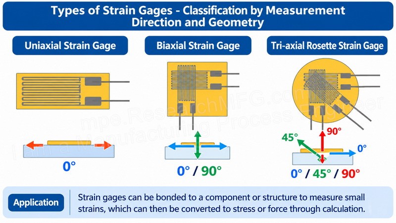
-
Uniaxial (Linear): Measures strain in one direction only.
-
Biaxial (90° Rosette): Measures strain in two perpendicular directions.
-
Three-element rosette (0°/45°/90° or 0°/60°/120°): Measures strain in three directions, allowing the magnitude and direction of the principal strains to be calculated. It is particularly useful when the principal strain direction is unknown.
-
Shear strain gage: Specifically designed to measure shear strain.
3. Other Classifications
-
Installation method: Bonded, welded, sprayed, or embedded strain gages.
-
Self-temperature-compensated (STC) strain gages: Designed to compensate for thermal expansion based on the coefficient of thermal expansion of a specific material.
-
Special-purpose strain gages: High-temperature, low-temperature, waterproof, and fatigue-resistant types, among others.
Strain Gages Suitable for PCB Applications
PCB (Printed Circuit Board) strain measurement has some special requirements. Available space is extremely limited, heat dissipation is relatively poor, and the PCB’s coefficient of thermal expansion (CTE) is typically around 13–17 × 10⁻⁶/°C. Measurements also often need to comply with standards such as IPC/JEDEC-9704, which covers strain measurement during assembly, board bending, drop testing, and thermal cycling.
Recommended Types
1. Miniature Metal Foil Strain Gages (Most Commonly Used)
-
Features: Very short grid lengths (0.2–2 mm), backing dimensions of approximately 1–3 mm, and commonly available in 120 Ω or 350 Ω resistance values.
-
The thermal expansion characteristics should be suitable for the PCB material (approximately 13 × 10⁻⁶/°C).
-
Available with a wide range of self-temperature compensation (STC), commonly from –30°C to 120°C or higher.
-
Representative products include:
-
Kyowa KFRS Series (designed specifically for printed circuit boards).
-
Micro-Measurements (Vishay) C2K / S5198 / G1350 Series (miniature planar rosette strain gages).
-
Other manufacturers, such as ZEMIC, also offer PCB-specific products, including certain ZF/BF series.
-
2. Miniature Three-Element Rosette Strain Gages
-
These are commonly used because the principal strain direction on a PCB is often unknown.
-
They measure strain in three directions simultaneously, allowing the principal strain magnitude and direction to be calculated.
-
The grid length is typically 1–2 mm or less, making them suitable for installation near component corners or BGA packages.
3. 350 Ω Strain Gages Are Generally Preferred Over 120 Ω Types
-
PCBs have relatively poor heat dissipation. Higher-resistance strain gages generate less self-heating and can generally tolerate a higher excitation voltage without compromising measurement accuracy.
4. Semiconductor Strain Gages (Less Common for General PCB Testing)
-
These are considered mainly when extremely high sensitivity or very limited installation space is required. However, temperature compensation is more difficult, so they are generally not the first choice for conventional PCB strain testing.
Practical Recommendations for PCB Testing
-
Choose a miniature metal foil three-element rosette strain gage, preferably with a grid length of 0.5–1.5 mm.
-
Install the gages near the four corners of the component or at other critical locations. According to JEDEC recommendations, the measurement location is approximately 3.5 mm from the component edge.
-
Use a fast-curing adhesive, such as cyanoacrylate, and carefully prepare the PCB surface by removing the solder mask where necessary, lightly abrading the surface, and cleaning it before bonding the gage.
-
The excitation voltage (also called drive voltage or operating voltage) is typically limited to 2–5 V or less to prevent self-heating.
-
Use a strain measurement instrument with a sufficiently high sampling rate, typically 500–2,000 Hz, to capture dynamic events.
-
During actual testing, it is recommended to record both temperature and strain rate so that the results can be properly compared with the allowable strain limits provided by the component manufacturer.
In summary: Standard metal foil strain gages are generally sufficient for conventional structural testing. However, miniature metal foil strain gages, especially three-element rosettes, are the most common choice for PCB strain measurement. Their small size, suitable thermal characteristics, stability, and reliability make them well suited to electronics assembly applications and industry testing requirements.
Related Articles
- [Case Study] BGA Solder Ball Cracking: Strain Gauge Analysis and Design Improvement
- BGA Solder Ball Crack Analysis: How to Identify the Root Cause Using the Red Dye Penetration Test




Leave a Reply