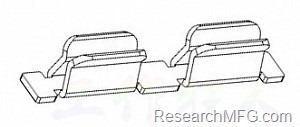
 Recently one of my top manager ask to mount the shielding-can or call shielding-cover directly on the Printed Circuit Board to instead of mount the shielding-clip or call shielding-frame on the board first then cover the shieling-can. He said this “new process” is more cheap and can reach better RF (Radiation Frequency) performance. Also most of current popular cell phone board apply this solution.
Well, I must say yes. Directly mount the shielding-can on the board is cheaper and save labor hours as compare it with mount one component (frame or clip) on the board first then install another component (can or cover) to cover it. But this new requirement also got lots of negative feedback from SMT factory and repair center. Because of directly mount shielding-can on board means that repair guy must de-solder the shielding can first before repair the component under the shielding can. It make the repair job more difficult and may give more trouble and damage the board during repair.
Related article: The benefit to use shielding clips to instead of shielding frame
Here WorkingBear would like to summary the pros and cons items of directly mount the shielding-can on board for your reference:
The advantage to directly mount the shielding-can on the board
-
Cost saving for material. I must say this solution is really cost saving. It save one component at least. This process no need to place the shielding-clip or shielding-frame component.
-
Labor hours saving. It also save the labor hours without install the shielding-can on clip or frame again since it already mount by SMT solution.
-
It may have chance to reduce the PCB warpage. Base on the mechanical design and PCB thickness. The shielding-can is metal material and may help to enhance the strength of PCB to prevent it from warpage during reflow process. Be noticed that If you really like to use the shielding-can to enhance the PCB stiffness to improve the BGA solder crack then you better consider to change the forming of shielding-can from stamping to drawing process.
-
RF performance improvement. As experience show that apply shielding-frame may get 2db RF performance better than shielding-clip. So directly mount the shielding-can on the board shall be also get better RF performance than shielding-clip. By the way, this RF performance shall base on the ability of RF engineer.
The disadvantage to directly mount the shielding-can on the board
-
There must be a AOI (Auto Optical Inspection) machine before reflow process and before the shielding-can placement. This is in order to inspect the SMD components placement quality under the shielding-can to reduce the soldering defect rate and minimum the repair percentage. Because of the components under the shielding-can can’t be optical inspection after reflow. For most of the SMT production line, this will increase one station and spend more resource.
-
The soldering quality may be risk under the shielding-can. Because of most of the shielding-can be designed as closed zone. The thermal transfer to inside the shielding-can will need more time. That means the reflow temperature profile setting window will be narrow. The soldering skip, tombstone, soldering short defect may be increased. By the way, no recommend putting the BGA or QFN components under the shielding-can since this kind of soldering under component body need more critical temperature control.
-
The co-planarity/flatness dimension is hard to control for the shielding-can component. Especially for the bigger size of shielding-can. Most of the SMT line ask the co-planarity/flatness shall be less than 0.1mm. Because of most of the stencil thickness is 0.1mm only. Sometimes we can apply the step-down or step-up stencil to partially increase stencil thickness but it will be 0.127mm maximum only. We must consider shielding can deformation during reflow high temperature factor. So 0.1mm maximum is the requirement for the co-planarity to guarantee its good solderability.
-
The test coverage will be low. The shielding-can will cover lots of the PCB and components. The AOI can’t inspect the components and solderability under shielding-can. Although we can implement one more AOI machine before reflow process to minimum the defect , but it still can’t guarantee there will be good solderability. By the way, directly mount shielding-can will also make reduce the test points quantity. Besides, the test points can move out from the shielding-can area.
-
The board level repair will become more difficult. Directly mount shielding-can is not only affect to debug efficiency but also make the repair more difficult. The average labor hour is 15~20 minutes by removing the shielding-can and re-mount the shielding-can. The repair guy even can’t guarantee the repair quality is good for the shielding-can and its adjacent components. Mostly of the condition will directly scrap the bad board.
Here is the labor hours and material cost comparison between shielding-clip and directly mount shielding-can/cover on board
Below table call shielding-can directly mount on board as “one component” and mount Shielding-clip or shielding-frame then install shielding-can as “two components”。
| ($USD) | One component | Two components |
| Assembly labor cost | 0 | 0.0253 |
| Repair labor cost (Suppose the repair rate is 0.2%) | 0.0065 | 0 |
| Repair material cost (Suppose the scrap rate is 0.4%) | 0.0002 | 0 |
| Sub-total | 0.0067 | 0.0253 |
Related article:
How EMS fabricate a PCB Assembly?
Selectively increase solder paste volume solutions
Solder Preforms – Another Choice for Solder Volume Increasing


Leave a Reply