

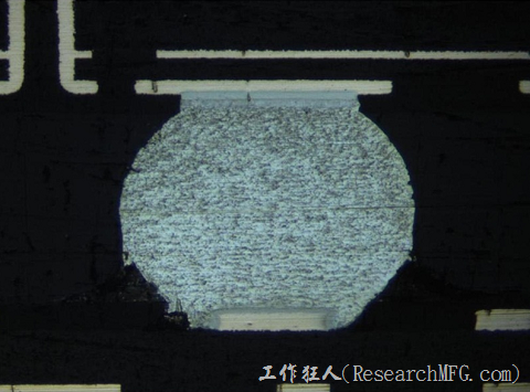
This article is intended for anyone who isn’t yet familiar with how to evaluate the quality of BGA solder joints from cross-section images.
Workingbear happens to have several cross-sectional photos from actual production boards that make excellent teaching examples. Among them are some very typical defects, including Head-in-Pillow (HIP) solder joints and solder balls that were stretched during assembly, resulting in weak solder connections.
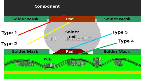
When you first look at a BGA cross-section, the first thing you should determine is which side belongs to the BGA package substrate and which side belongs to the PCB.
My preferred method is to compare the copper foil thickness. The side with the thicker copper foil is usually the PCB because BGA package substrates are generally much thinner than printed circuit boards and therefore use thinner copper layers. So, could you identify which site is the BGA substrate
If the cross-section clearly shows a Head-in-Pillow (HIP) defect—as shown in the example below—another easy way to identify each side is by comparing the size of the two solder balls.

The larger solder ball is usually the original solder ball attached to the BGA package. It has already gone through one reflow cycle before assembly, so it retains most of its volume. The smaller solder ball comes from the solder paste printed on the PCB. During reflow, the flux evaporates, leaving behind only about half of the original solder paste volume.
Pad size, however, isn’t always a reliable indicator because it depends on the PCB pad design. For example, some manufacturers prefer using Copper Defined Pads (CDP), also known as Non-Solder Mask Defined (NSMD) pads.

Evaluating BGA Solder Joint Quality
Head-in-Pillow or Head-on-Pillow defect of BGA solder joint
The first example below shows a classic Head-in-Pillow (HIP) defect. If you’re unfamiliar with HIP, you can read my separate article discussing Head-in-Pillow defects in more detail.
Approximately 99% of HIP defects occur on the outermost row of BGA solder balls, especially at the four corners of the package.
The primary cause is package or PCB warpage during the reflow process. As the assembly heats up, either the PCB or the BGA substrate can warp enough to separate the molten solder ball from the molten solder paste. When the assembly cools, the board gradually returns to its original shape, but by then the solder has already solidified. The result is two solder balls touching each other without fully merging into one joint.
A HIP defect represents a serious soldering failure. Unfortunately, it is difficult to detect using standard 2D X-ray inspection or functional testing, which means defective products may reach customers. After a period of use, intermittent electrical failures begin to appear, and the products are eventually returned for repair. (HIP defects can be detected using a 2.5D X-ray system, which allows the PCB to be tilted and rotated during inspection. This makes it possible to observe the BGA solder joints from an oblique angle and identify the characteristic double-ball structure.)
Poor BGA solder joint
The second example represents a solder joint that falls somewhere between a normal joint and a complete HIP defect.
Now that you know how to identify the PCB side, take a closer look at the image below.
The BGA solder ball and the PCB solder paste have completely fused together, so there is no longer a visible double-ball structure. However, the entire solder joint appears vertically stretched and shows signs of nearly cracking apart.
Looking at the PCB side, you’ll also notice that the solder contact area on the PCB pad is relatively small, and the joint forms an unusual angle.
One possible explanation is that the PCB uses an SMD (Solder Mask Defined) pad design. In this design, the solder mask overlaps the edge of the copper pad, reducing the available solderable area.
The downside of SMD pads is reduced solder joint strength. Under vibration or repeated thermal expansion and contraction caused by power cycling, cracks are more likely to develop at the solder joint.

Acceptable BGA solder joint
The solder joint shown in the next image would generally be considered acceptable.
The solder ball has collapsed properly during reflow, forming a slightly flattened, oval-shaped joint. However, you can still see that the solder wetting area on the PCB side is smaller than that on the BGA substrate side. A sharp angle also forms where the solder meets the PCB pad, creating a potential stress concentration point.
This again appears to be the result of an SMD pad design, which limits the solderable area.
Recommend reading:
- Why BGA soldering ball always crack(1)? Stress > bonding-force
- Differences, advantages, disadvantages, and recommendations for SMD and NSMD pad designs

The High-quality BGA solder joint
Ideally, a high-quality BGA solder joint should look more like the example below.
The solder joint resembles a small lantern, with the solder fully wrapping around the entire PCB pad.
When NSMD (Non-Solder Mask Defined) pads are used, the solder can wet the entire copper pad without being restricted by the solder mask, producing stronger solder joints.
However, there is always a tradeoff.
Because NSMD pads expose more copper, the actual copper pad is slightly smaller than an equivalent SMD pad. This reduces the pad’s bonding strength to the PCB laminate, making pad adhesion another important design consideration.
For this reason, there is no universal answer as to whether SMD or NSMD is the better choice. The appropriate pad design depends on the product requirements, PCB construction, reliability goals, and manufacturing considerations.
If you actually discover cracked BGA solder joints, the analysis becomes much more involved.
Workingbear has written an entire series of articles covering BGA solder joint cracking and component detachment failures. If you’re interested in learning more about failure mechanisms and root cause analysis, be sure to check out those articles as well.
Related Posts:



Leave a Reply