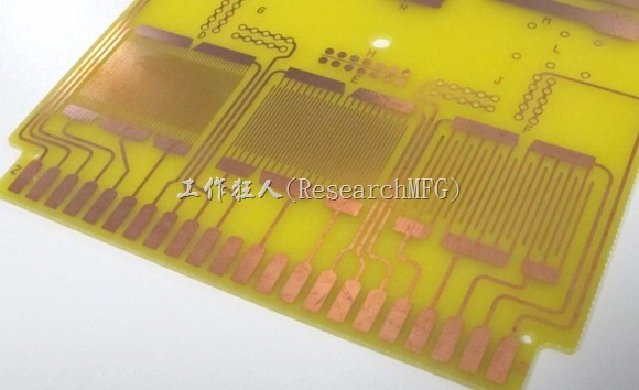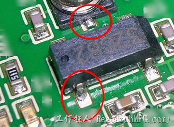
This is just a summary article about PCB surface finishes. Workingbear has only worked on the electronic system assembly factory and has not been involved in the production process of bare PCBs. Therefore, the following insights are based on personal opinions. If you have different opinions or notices any mistakes, please feel free to comment and engage in discussion.
The main purpose of PCB surface finishes or call treatment is to protect the copper layer on the surface of PCB from direct contact with air, and prevent oxidation.It also facilitates effective soldering, whether directly or indirectly, with the solder, ensuring electrical conductively attaching electronic components.
With the evolution of technology and the increasing demand for environmental protection, the electronic industry has been actively or passively advancing with the times, and the technology of PCBs has also been evolving. The following are several common PCB surface finishing processes in the industry. Workingbear can only say that there is no perfect surface finishing process currently available, which is why there are so many options. Each surface finish process has its own advantages and disadvantages, which are listed and explained below.
Bare Copper Board
As the name suggests, “bare copper board” refers to the copper foil surface of the PCB without any surface finish or protection. The outermost layer of the circuit is completely exposed and comes into direct contact with atmosphere once it is unpacked.
Advantages of bare copper board:
Low cost, high surface flatness, good solderability (note: under the condition of no oxidation yet).
Disadvantages of bare copper board:
Because there is no surface protection, it is vulnerable to acid and humidity and cannot be stored for a long time. It must be used within 2 hours after unpacking, because the copper is easily oxidized when exposed to atmosphere.
It cannot be used in double-sided reflow processes because the second side will already be oxidized after the first reflow soldering.
If there are test points, solder paste must be added to prevent continued oxidation, otherwise subsequent contact with the probe will not be good.
HASL (Hot Air Solder Leveling)
HASL, commonly known as PCB spray tin, is a process in which a layer of tin is sprayed onto the surface of the copper foil to protect it, and then the surface is flattened using a hot air knife. The commonly used equipment for tin-spraying can be roughly divided into two types: vertical and horizontal, each with its own advantages and disadvantages.
Advantages of HASL PCB:
Fresh tin can achieve better wetting effect because the coating itself is tin and solder paste is tin base too. Compared to ENIG, the cost of HASL is lower, but the cost is higher than OSP. The soldering performance of HASL PCB is also good, but this is usually only applicable to the first reflow. It is not necessarily an advantage for the second reflow side.
Disadvantages of tin-sprayed PCB:
It is not suitable for soldering fine-pitch and small size components because the surface flatness of HASL PCB is poor, especially when it comes to the second reflow side, which has undergone one reflow already. The surface tin may melt again after the first reflow, which will cause the flatness of the solder pad to become worse. Of course, this can be overcome by the thickness of the solder paste, but don’t forget that too thick of a solder paste is not recommended for fine-pitch components.
During the PCB Assembly process, it is easy to produce solder beads, which can cause solder short for fine-pitch components. When used in double-sided SMT processes, because the second side has already undergone the high-temperature reflow of the first side, it is extremely easy for the spray tin to melt again and form solder beads or droplets affected by gravity, resulting in a less flat surface and affecting soldering problems.
In addition, the second reflow side may also experience tin oxidation and IMC thickening during the first reflow, which can consume the tin layer and affect the solderability, especially on thinner tin-sprayed boards.
Solder bridging due to droplets affected.
ENIG (Electroless Nickel Immersion Gold)
ENIG is a process that applies a layer of “nickel” onto the surface of copper foil using chemical methods, followed by a layer of “gold”. The purpose of the gold in ENIG is only to protect the nickel layer from oxidizing upon contact with atmosphere and affecting the quality of the solder in the future.
Advantages of ENIG boards:
Less prone to oxidation, can be stored for a long time, and has a flat surface, making it suitable for soldering small size components with fine pitch. It is the preferred choice for contact button circuit (such as mobile phone boards).
It can be subjected to multiple reflow soldering without significantly reducing its solderability.
It can also be used as a substrate for COB (Chip On Board) wire bonding, but a certain thickness of gold layer is required.
The reason why ENIG is less prone to oxidation is because the surface gold layer protects the underlying nickel layer, so the thickness of the gold layer is important. If the gold layer is too thin, it cannot protect the nickel, but if it is too thick, it can hinder the formation of nickel-tin alloys.
Disadvantages of ENIG boards:
Higher cost and poorer soldering strength because the IMC is a tin-nickel alloy as compare with tin-copper alloy. Moreover, using the electroless nickel plating process can easily lead to black pad problems. The nickel layer will oxidize over time, which can be a reliability issue in the long run.
OSP (Organic Soldering Preservative)
OSP is a surface finish process that uses a chemical method to grow an organic protectant on the surface of copper. This layer of organic protectant can be easily removed by solder flux at high temperatures, exposing a clean copper surface that can be wetted with solder paste. The thicker the organic protectant layer, the better the protection for the copper foil, but it also requires a more active solder flux to remove it for soldering.
Advantages of OSP boards:
Affordable: Among various PCB surface finishes, OSP is the cheapest, except for being slightly more expensive than bare copper boards.
Has all the advantages of bare copper boards: Fresh boards have good solderability, and expired boards (three or six months) can be reprocessed, usually limited to one reprocessing, depending on the presence of fine traces or pads on the surface. Reprocessing may etch a small amount of copper, making it unsuitable for too fine circuits.
The copper-based OSP has good solder strength for fresh OSP solder joints, and can withstand greater impact stress. The solder strength of fresh copper-based OSP is better than that of nickel-based OSP, but it will degrade over time. (For more information, read: Comparison of OSP and ENIG surface-treated circuit boards with data on the strength of solder joints)
Disadvantages of OSP boards:
Easily attacked by acid and moisture, affecting the protection of the copper surface. When used in secondary reflow soldering, it needs to be completed within a certain time frame. Generally, the effect of the second reflow soldering will be worse. In addition, if the storage time of the OSP board exceeds three or six months, surface treatment must be performed again. Detailed information may need to be obtained from the original board manufacturer regarding the storage period that can be tolerated by the OSP material used. Generally, the package must be used within 24 hours after opening.
The OSP film is an insulating layer, so test points must be printed with solder paste to remove the original OSP film for needle contact for electrical testing.
OSP boards cannot be used as surface finishes for button contacts because the copper protectant film cannot withstand too many button friction movements, causing exposed copper and poor contact after oxidation over time.
In addition, OSP boards are copper-based, and after soldering, they initially generate benign IMC (Cu6Sn5). However, over time, they will gradually generate inferior IMC (Cu3Sn), causing reliability issues. Therefore, if long-term use in high-temperature environments or products with longer lifespans is required, the long-term reliability issues of OSP must be considered.
Immersion silver, Im-Ag
First of all, Workingbear have no personal experience with the use of immersion silver for PCB surface finish. Therefore, the following information regarding immersion silver is based on what I have heard from my relatives and my own thoughts. Please take this as a reference only and feel free to correct me if you are an expert in this field.
The process of surface finish with immersion silver is quite simple. It utilizes the Giovanni effect principle, which directly replaces the surface copper (Cu) of PCB with silver (Ag) through the following reaction:
2Ag+ + Cu → 2Ag + Cu2+
Under normal conditions, copper has a higher potential and thus loses electrons, resulting in oxidation (Cu –> 2e– + Cu2+). On the other hand, silver has a lower potential and gains electrons, leading to reduction (2Ag+ + 2e– –> 2Ag).
Advantages of silver immersion include:
Since the surface silver is replaced by deposition, the surface is smooth, similar to immersion gold. Furthermore, the price of silver should be lower than that of gold.
Silver can improve the wettability of soldering and enhance the strength and fatigue resistance of solder joints. However, if the content of silver is too high (weight ratio over 4%), the solder joint may become brittle, which needs to be paid attention to.
Although silver also reacts with tin to form IMC Ag3Sn under high heat, this layer of silver is very thin and should play a role in protecting the underlying copper from oxidation, similar to gold (Au) in ENIG. Therefore, the actual IMC after soldering should still be tin-copper alloy.
Disadvantages of silver immersion include:
Based on Workingbear’s understanding, immersion silver was only popular for a period when RoHS was first implemented, and fewer people have used it later.
If the content of silver in the solder exceeds a certain ratio, tin whiskers may easily grow during the soldering process. During use, there is also a risk of electromigration and dendrite growth, which may cause quality issues, particularly for products with fine pitch.
It is also rumored that tiny bubbles may form beneath the IMC layer due to immersion silver , which may affect the reliability of products, especially BGA components.
Immersion silver is easily affected by environmental pollution and sulfuration when placed in the atmosphere, which may affect appearance and soldering quality. It is generally recommended to use it within 48 hours after opening.
This article translate from 電路板表面處理的目的?整理幾種常見PCB finish的優缺點
Related Articles:


Leave a Reply