

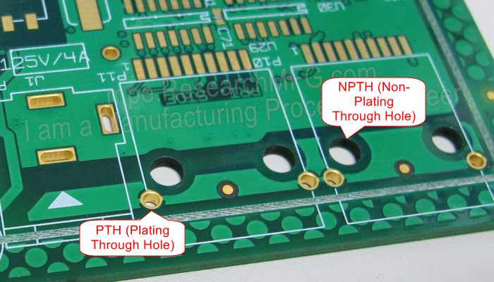
If you ever get the chance to hold a printed circuit board (PCB) in your hands and take a closer look, you’ll notice there are many different-sized holes. When you hold it up to the light, you’ll even see lots of tiny holes that let the light shine through. These holes aren’t just there for looks – each one serves a specific purpose. Generally, the more holes locate on the PCB, the more expensive it is to make the PCB.
These holes on the PCB can be divided into two main types: Plating Through Holes (PTHs) and Non-Plating Through Holes (NPTHs). The term “through hole” is used because these holes go all the way through the PCB, from one side to the other. Besides the through holes, there are also other holes on the PCB that don’t go all the way through. If you’re interested, you can check out this article: What is blind hole, buried hole and plating hole for PCB?
How can we tell the difference between PTH (Plating Through Hole) and NPTH (Non-Plating Through Hole)?
It’s actually quite easy. Just take a look at the picture at the beginning of the article and check if there are shiny metal plating on the vertical walls of the holes. If there are, then it’s a PTH. If there are no plating marks, then it’s an NPTH.
What are NPTH (Non-Plating Through Hole) used for? If you pay close attention, you’ll notice that NPTHs are usually larger in diameter compared to PTHs. Most NPTHs are designed for screwing the PCB onto the casing. Some NPTHs are used for mounting and providing alignment I/O connectors on the PCB, even structural support. Others are used for mechanical interlocking purposes.
Additionally, some PCBs may have NPTHs along the board edge (break-away, coupon) to serve as markers for testing fixtures. In the past, these NPTHs were also used to hold the PCB in place during SMT process, but nowadays, most SMT machines use clamps instead. However, for thinner boards, NPTHs may still be necessary to prevent deformation during assembly.
What are PTH (Plating Through Hole) and vias used for?
PTHs on a PCB have two main purposes. One is to solder Through Hole Devices (THDs), which have pins that go through the plating holes and are soldered to the PCB. These holes diameter need to be bigger than the device’s pins to accommodate the soldering process.
Vias, on the other hand, are smaller holes that serve a different purpose. They are used to connect and carry electrical signals between different copper layers on the PCB. PCBs are made up of multiple layers of copper, separated by insulating layers. Vias act as pathways that allow signals to travel between these copper layers. Think of them as staircases connecting different floors of a building. They enable communication between the copper layers.
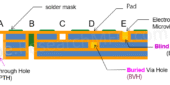
The diagram on the left shows a cross-section of a PCB. Imagine it as a nest of ants inside a glass jar. This particular PCB has six layers of copper foils, like a building with six floors. Each copper layer represents a floor, and the vias are like staircases that connect different floors. Some staircases only connect the third and fourth floors, while others have different connections. These specific vias are called “Buried Via Holes” because you can’t see them from the outside of PCB. Vias are used to connect different layers of copper, and they need plating to work. They are a type of PTH.
Nowadays, most vias are covered with solder mask, as shown in the left diagram. This protective coating insulates the vias. It is especially important for mobile phone boards where components are located closely together. Some vias might be located right beneath components. To prevent potential solder bridge between components and vias, which could cause quality or functional issues, a solder mask is applied to cover the vias.
Another reason for using a solder mask to cover vias is to prevent melting solder paste from flowing through the vias during the reflow process. This could lead to solder short. Therefore, more PCB reduce the vias diameter and apply a solder mask upon it.
Certainly, using solder mask to cover vias may be seen as having quality risks because there could be incomplete coverage or the potential for residual chemicals causing corrosion. However, it’s important to note that using solder mask is currently the most cost-effective and widely accepted method for filling vias.
In addition to solder mask plugging, some PCB processes first fill the vias with resin and then cover the surface with solder mask. This approach generally provides better quality and reliability, but it adds an extra process step and therefore increases the cost.
When a via is located in an area where surface-mount components will be soldered, VIPPO (Via-In-Pad Plated Over) can be used. In this process, the via is first filled with resin and then plated over with copper, completely sealing the via and reducing the risk of solder paste flowing into the via during reflow.
However, based on practical experience, even when VIPPO is used for BGA pads, small voids can still remain inside the resin fill. During reflow, these voids may expand due to thermal expansion or trapped gas, causing the solder joint to bulge locally. This can increase the risk of bridging with adjacent solder balls and may also affect solder joint reliability.
Therefore, if the cost is acceptable, Workingbear generally recommends using copper electroplating for via filling for through-holes or blind vias located in BGA pads (via-in-pad). Filling the via directly with electroplated copper can reduce the risk of voids associated with resin filling and further improve BGA solder joint reliability.
Related Article:
- The Hidden Dangers of Using Overdue PCBs: Can Baking Salvage Them?
- For Beginners: What Is a BOM? How BOM Works with ECO, ECN, and ECR in Electronics Manufacturing
- What is the Purpose of Surface Finishes for PCB? A Summary of the Pros and Cons of Common PCB Finishes
- What are ICT(In-Circuit Test) and MDA(Manufacturing Defect Analyzer) in Electronics Manufacturing? Any Benefits?
- How to Bake PCB? Baking Conditions and Methods, Why Expired PCBs Need to Be Baked Before SMT or Reflow Soldering?


Leave a Reply