The primary purpose of adding Nitrogen (N2) to the SMT reflow oven is to reduce oxidation on the soldering surface and improve the wettability of the solder joints. Nitrogen is a colorless, odorless, and chemically inactive gas. It belongs to the category of inert gases, meaning it doesn’t easily react with most metals to form compounds. By using nitrogen to replace the oxygen in the environment, we can prevent metals from reacting with oxygen, thus avoiding oxidation.
(This is a summary article, and the views expressed may not be entirely accurate. If you find any issues, feel free to share your opinions or feedback.)
Note: Workingbear did some research and found that Nitrogen (N2) is classified as an “inert gas” in modern chemistry. Additionally, Group 18 elements (8A) on the periodic table, including helium (He), neon (Ne), argon (Ar), krypton (Kr), xenon (Xe), and radon (Rn), are called “noble gases.” Inert gases include both nitrogen and noble gases.
The reason nitrogen can improve soldering performance for surface mount is that “the surface tension of solder in a nitrogen environment is lower than when exposed to the atmosphere.” This leads to better solder flow and improved wettability. Moreover, nitrogen reduces the concentration of oxygen (O2) and other contaminants that can pollute the soldering surface, significantly lowering oxidation during high-temperature soldering. This is especially beneficial for improving the quality of reflow soldering on the second side of the board.
When a printed circuit board (PCB) goes through reflow oven on the first side (1st side), the surface finish on the second side is also exposed to high temperatures, which may damage it, especially if the PCB uses OSP surface finish. Oxidation can rapidly occur in high-temperature environments. By adding nitrogen, oxidation on the second side can be greatly reduced during the first reflow, helping to ensure the best soldering performance during the second reflow.
Additionally, if the partially assembled PCBA is left exposed to air for too long between the first and second reflow processes, oxidation can occur on the second side, leading to issues like solder rejection or insufficient soldering during the second reflow.
This is where the advantages of ENIG PCB become apparent. Since the surface finish for ENIG is gold (Au), oxidation is almost non-existent at current reflow temperatures on the second side. However, for HASL or Im-Sn PCBs, the high temperature of the first reflow causes IMC to form prematurely on the second side before it has even been soldered, affecting the reliability of the second reflow.
For those interested in ENIG and HASL and Im-Sn PCBs, you can refer to some related articles on Workingbear’s blog:
-
Two Major Issues with ENIG PCB Pads (Black Nickel and Phosphorus Layer) and Preventative Measures
However, Workingbear must emphasize that “nitrogen is not a cure-all for PCB oxidation.” If the components or the surface of the PCB are already severely oxidized, nitrogen won’t magically restore them. It can only provide a remedial effect on slight oxidation. Remember, it’s a remedy, not a solution. In reality, as long as the PCB surface finish and components can be properly stored and handled to prevent oxidation, adding nitrogen doesn’t make a huge difference. At most, it improves solder flow and increases solder wetting height. That said, it’s rare to find companies that can guarantee their PCBs and component surfaces are 100% oxidation-free.
We’ve discussed many benefits of adding nitrogen during reflow, but let’s not forget that using nitrogen in a reflow oven isn’t without its downsides. Apart from the cost of using nitrogen, the fact that it enhances solder flow can sometimes create problems. How does that sound strange?
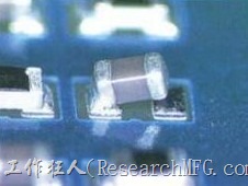
 Tombstoning of resistors and capacitors can occur when solder flows too well, leading to better wetting. This effect is generally beneficial for most components, but it can worsen the “Tombstone effect” in small-chip components like resistors and capacitors. One end of the component may start melting before the other, and once the first end melts, the stronger cohesion may begin pulling the component up. Since the unmelted end lacks enough cohesion to hold the component down, it can cause it to stand upright, forming a tombstone. Based on experience, tombstoning is particularly prone to occur with small resistors and capacitors like 0603 and 0805 sizes, especially capacitors, due to their size and the spacing between solder paste deposits.
(Additional clarification: The previous paragraph may have caused some confusion, so here’s a clearer explanation. The reason nitrogen can worsen the tombstone effect is that nitrogen accelerates the wetting speed of the solder paste once it melts. This causes some solder joints to wet prematurely, increasing the time difference between the soldering of both ends of the component. Ultimately, this difference in timing creates an imbalance in forces on either side of the component, leading to tombstoning. This should clarify how nitrogen influences the tombstone effect!)
Moreover, nitrogen also increases the “capillary effect” of solder, allowing it to climb higher along the surface of component leads. This may be beneficial for some components, but it can be a disadvantage for certain connectors. As the solder climbs higher up the connector leads, it may reach the contact points connecting to other components. If these contact points become contaminated with solder, it could lead to connectivity issues. Additionally, modern connectors have very narrow pin spacing, and solder climbing up could increase the risk of short circuits. If all the solder climbs up the leads, it could leave the pads on the board with insufficient solder, eventually leading to the “Solder Wicking Effect” and resulting in poor or incomplete solder joints.
Let’s summarize the key points from earlier
Advantages of using nitrogen in a reflow oven:
-
Reduces oxidation during reflow.
-
Improves soldering performance.
-
Enhances solder wettability.
-
Reduces the void rate because oxidation on solder paste or pads is minimized, improving solder flow, which naturally reduces voids. However, this may only apply to solder joints with smaller amounts of solder. For BGA solder balls, which involve a larger volume of solder, it may have the opposite effect.
Disadvantages of using nitrogen in a reflow oven:
-
Expensive.
-
Increases the likelihood of tombstoning defects.
-
Enhances the capillary effect (solder wicking).
-
When using nitrogen, be mindful of whether tombstoning defects are increasing, and also check whether solder wicking on connector leads is rising and affecting contact points.
-
Additional note: It may increase void rates in BGA solder joints.
Theoretically, adding nitrogen (N2) in a reflow oven can reduce the surface tension of both the solder paste and the metal being soldered. Lower surface tension helps the solder powder spread and allows flux gases to escape, thus reducing voids. However, the impact of surface tension on voids depends on the type of solder joint:
-
Non-BGA solder joints (those with smaller amounts of solder): Solder collapse is less likely, and lower surface tension helps the solder powder migrate and spread on the metal, reducing solder voids. In other words, it improves wetting on the metal being soldered or on the solder pads, lowering non-wetting-related voids.
-
BGA solder joints (those with larger and thicker amounts of solder): Lower surface tension may not sufficiently support the liquid solder, allowing gases to gather more easily during the soldering process, which can lead to larger voids.
For more detailed information, you can refer to the article “Effects of Nitrogen (N2) in SMT Reflow on Various Soldering Defects.”
What kinds of PCBs or components are suitable for nitrogen reflow?
-
OSP surface-finished double-sided reflow boards are suitable for nitrogen use.
-
Use nitrogen when components or PCBs show poor solderability. For example, it can enhance wetting on the sides of QFN or Castellated Terminations.
-
Large package and high-density BGA, but be mindful of the potential increase in void rate.
Related Post:


Leave a Reply