Working for manufacturer engineering couple years. Sharing the manufacturing experience, skill, DFx, design, and information. Be care of this blog is personal share and content may not be 100% correctly.
Figure 1: How to interpret the deeper meaning of a laboratory BGA red dye penetration test report
If I showed you the microscope image above (Figure 1), taken right after a Red Dye Penetration Test, could you tell Workingbear what happened to the solder joints on this BGA? Actually, Figure 1 has already used red boxes to point out where the solder balls cracked. But beyond that, how much of the story behind the failure can you figure out?
Over the past few days, Workingbear has been analyzing quite a few BGA Red Dye Penetration Test results. It almost feels like everyone agreed to send them in at the same time. Suddenly, we have multiple different products and PCBAs, all with BGA-related issues.
While discussing the red dye test results and possible root causes with other departments, I realized that quite a few people still don’t really know how to read a red dye test report from a laboratory.
So today, let’s take a closer look at how to understand what the laboratory’s red dye penetration test report is actually telling us.
Workingbear has summarized several key points that many people have difficulty understanding when reading a red dye test report:
1. Not Knowing Where Pin 1 Is on the BGA Component and PCB
Pin 1 is extremely important. If you don’t know where Pin 1 is, how can you determine where the cracked solder ball is located on the PCB? And how can you determine the possible effect of mechanical stress on the PCB and BGA?
Normally, the Pin 1 location should be marked on the PCB silkscreen. Some boards use a dot, while others use a triangle. However, in this particular photo, the Pin 1 marking on the PCB happens to be covered by red dye. If possible, I recommend comparing it with another board that has not been subjected to the red dye test so you can confirm the exact Pin 1 location.
For the BGA component itself, as shown on the right side of Figure 2 below, the Pin 1 location is typically indicated by a small triangle on the component side. There is also usually a dot or other marking on the top of the BGA package to indicate Pin 1.
Figure 2: Pin 1 location is critical when analyzing BGA solder ball failures
2. Not Knowing the Relative Location of the Cracked Solder Ball or the Direction of Crack Propagation
The crack pattern in BGA solder balls can often provide clues about the direction of the applied stress. In general, the solder balls closest to the stress source tend to show more severe cracking, while the cracks become less severe as the stress propagates toward the center of the BGA.
For example, if the solder balls near one corner or edge of the BGA are completely cracked, while the cracks become smaller or disappear as they move toward the center, this pattern suggests that the stress was introduced from that corner or edge and propagated inward. The red dye penetration test can help reveal this crack pattern by showing which solder balls are fully cracked, partially cracked, or unaffected.
3. Determining Whether the Solder Ball Cracked on the Component Side or the PCB Side Is Critical
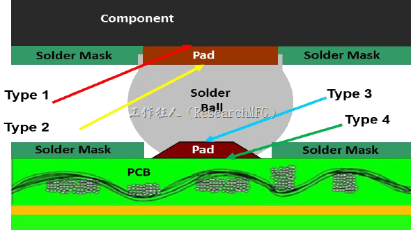
If the solder ball fracture occurs on the component side, it usually means the problem is less likely to be related to the SMT assembly process. The solder balls were already attached to the BGA component before the component arrived at the factory. Therefore, if there is a problem, it is most likely related to mechanical stress. In a smaller number of cases where the problem is related to soldering, it may be a quality issue originating from the BGA component supplier.
However, there is one important exception. If the BGA has previously been reworked or reballed, the problem could be related to the SMT process. A professional EMS (Electronic Manufacturing Services) factory should have records of this type of repair or rework history.
If the solder ball fracture occurs on the PCB side, the first thing to check is whether the solder pad was pulled up together with the solder ball. If it was, this usually indicates that the solder joint itself had good solderability and that the solder joint strength was actually greater than the bonding strength between the PCB pad and the PCB laminate. In this case, the problem is more likely to be related to mechanical stress or insufficient pad adhesion to the PCB.
If the PCB pad was not pulled off, the next thing to examine is the appearance of the fracture surface. A fracture caused by mechanical stress will generally show an irregular, rough-looking surface with signs of tearing or deformation.
Keep in mind that “rough” here is a relative description. A simple way to judge it is to hold the fractured solder ball under the light. If you cannot see a bright reflection from the fracture surface, it can generally be considered a rough surface.
If the fracture surface is rough, it often indicates that the crack occurred through the IMC (Intermetallic Compound), because the IMC layer is generally one of the most brittle regions in a BGA solder joint. When mechanical stress is applied, the crack tends to propagate through the weakest part of the structure—just like water naturally flows toward the lowest point.
On the other hand, if you observe the fracture under suitable lighting and the surface looks smooth and shiny, meaning that you can see a clear reflection, there is a good chance that the failure is related to a soldering defect such as HIP (Head-in-Pillow)/HoP (Head-on-Pillow) or NWO (Non-Wetting Open).
Of course, the best approach is to perform a cross-section and examine the formation of the IMC layer to confirm the soldering condition. In general, the IMC should form uniformly across the entire solder interface. You should not see areas where IMC has formed next to areas where there is little or no IMC. Non-uniform IMC formation can significantly reduce the solder joint’s ability to withstand mechanical stress.
4. How Can You Tell from the Image Whether the Solder Ball Cracked on the Component Side or PCB Side? Why Are Some Cracked Solder Balls Larger Than Others?
Figure 3: How to determine whether the solder ball fractured on the component side or PCB side
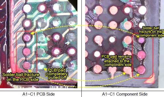
Let’s go back to Figure 1 at the top of this article and compare it with the annotated Figure 3. First, look at the image on the left side of Figure 3. This is the PCB-side view after the BGA red dye penetration test. The red boxes highlight three solder balls—A1, B1, and C1—that show signs of cracking. The round solder ball surfaces are stained with red dye, and the entire surface of each solder ball is covered with red dye. This indicates that the solder joints have completely fractured.
Looking more closely at the PCB-side image, you can see that the diameters of the A1 and B1 solder balls appear to be different from C1. C1 appears smaller. This is because the fracture surfaces of A1 and B1 are located on the PCB side, so what you are seeing is actually the diameter of the PCB solder pads. In contrast, the fracture surface of C1 is located on the component side, which makes the visible diameter smaller.
Generally speaking, for the same BGA solder joint, the PCB pad is larger than the pad on the BGA component. If you look carefully at the C1 solder ball on the PCB side, you should still be able to see a faint, blurred spherical shape underneath the fracture surface. Its size should be approximately the same as A1 and B1. This provides additional evidence that the C1 fracture occurred on the component side, because most of the solder ball remained attached to the PCB pad.
Next, let’s look at solder ball A2. In the PCB-side image on the left, A2 appears as a bright white circular area. This usually means that the PCB pad has been pulled off. In other words, when the BGA package was separated from the PCB, the PCB pad was torn off and remained attached to the solder ball. In the corresponding component-side image on the right, you can see the copper-colored PCB pad, including a small tail of copper, still attached to the solder ball on the BGA component.
Figure 4 below shows a PCB that was returned from the laboratory after the red dye penetration test. The PCB was tilted at an angle before the photo was taken. This makes it much easier to determine whether the solder balls remained attached to the PCB side or were pulled away from the PCB.
Figure 4: PCB photographed at an angle after the BGA red dye penetration test
Workingbear strongly recommends asking the laboratory to return both the PCB and the BGA components after completing the red dye penetration test. You should then examine them yourself under a microscope to verify whether the laboratory’s interpretation is correct.
You may also discover additional issues that were not identified in the original laboratory report. After all, nobody understands your own product better than you do.
Now, you should be able to understand what a laboratory red dye penetration test report is really telling you!
From this point on, you should be able to read the report and make your own judgment about why the BGA failed.
Workingbear is definitely not all-knowing. The amount of evidence determines the amount of confidence you should have in your conclusion. If the red dye test report cannot tell you something, asking me won’t magically give you the answer either. You need to perform additional tests and analyses.
And if the IMC inspection also shows no problems, then maybe the solder itself isn’t the problem. Don’t automatically point the finger at the factory and say, “Your soldering wasn’t done properly!” just because a BGA failed.
Finally, Workingbear would like to remind you of a few things:
Don’t just look at whether the solder balls have been stained with red dye. You also need to examine where the fracture occurred and what the fracture surface looks like.
When you only have a single sample, non-destructive inspection should generally be performed first.
The laboratory report should still be independently verified by your own engineering team.







Leave a Reply