Working for manufacturer engineering couple years. Sharing the manufacturing experience, skill, DFx, design, and information. Be care of this blog is personal share and content may not be 100% correctly.
Figure: Use the Red Dye Test to Identify BGA Solder Ball Cracks: Failure Patterns and Practical Analysis
BGA IC functional failures are a major headache for many electronics companies. This is especially true today, as most CPUs use BGA packages. When a product with a boot-up failure is returned from the customer and we need to determine the root cause, one of the most common methods used to identify the root cause is the Red Dye Penetration Test.
One of the main advantage of the Red Dye Test is that it provides a clear visual indication of where solder ball cracks have occurred across the entire BGA. This allows manufacturing and R&D engineers to quickly identify potential failure locations and better understand the possible causes and sources of mechanical stress.
Figure: Using the Red Dye Penetration Test to Detect Cracked BGA Solder Joints
However, the Red Dye Test is a destructive test. It is recommended that all feasible non-destructive analysis methods should be performed first, such as visual inspection, optical inspection, 2.5D or 3D CT X-ray, and ultrasonic inspection. The Red Dye Test should only be performed as a last resort when these non-destructive methods cannot provide enough information to identify the failure.
In theory, samples that have gone through a Red Dye Test can still be cross-sectioned for further SEM (Scanning Electron Microscope) imaging and EDX (Energy-Dispersive X-ray spectroscopy) elemental analysis. However, the sample has already been subjected to physical force during the Red Dye Test, and some areas may also have been contaminated by the red dye or other substances. In other words, the sample is no longer in its original, as-failed condition after the Red Dye Test. Therefore, any results obtained from subsequent analysis should be interpreted with caution.
Another limitation is that the Red Dye Test cannot determine whether there is a problem inside the PCB or BGA package. Some failures may be caused by broken vias or internal CAF (Conductive Anodic Filament) failures within the PCB and wire bond faiulre insides inside the BGA package. Once the Red Dye Test is performed, these failure features may be damaged, altered, or even lost, making it more difficult to identify the original failure mechanism.
Therefore, a more cautious approach is to start with electrical testing and try to identify which solder balls and signal paths may be involved. Then, step by step, narrow down the possible failure locations. Ideally, you should also determine whether the failure is an open circuit or a short circuit. Once the suspected area has been narrowed down, perform a cross-section directly to get to the root cause.
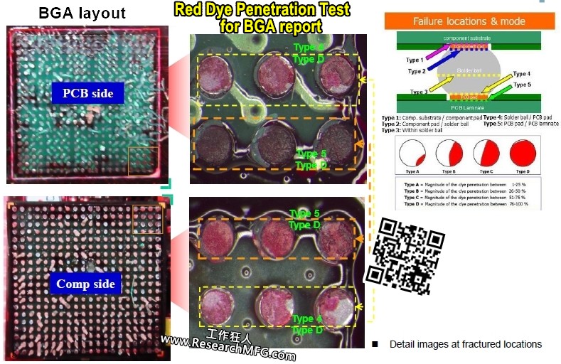
That said, for the purpose of this article, I will still use the Red Dye Test as the main method of explanation. The following is a typical report format used by laboratories after performing a Red Dye Test on a BGA. Different laboratories may use slightly different formats, but the basic way of presenting the results is generally very similar.
However, the Red Dye Test still has several advantages. It is relatively simple to perform, costs less than many other failure analysis methods, and allows us to examine the solder joints of all the solder balls on an entire BGA at once. Therefore, this article will use the Red Dye Test as the primary method of analysis. The following is a typical report format used by laboratories (labs) after performing a Red Dye Test. The format may vary slightly from one laboratory to another, but the overall classification and reporting methods are generally very similar.
BGA Red Dye Test Solder Ball Crack Types:
Figure: Use the Red Dye Test to Identify BGA Solder Ball Cracks: Failure Patterns and Practical Analysis
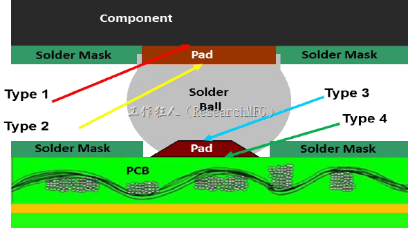
The diagram at the top shows the different BGA solder ball fracture locations. The following color-coded classification is used to indicate where the solder ball has separated. Please note that reports issued by different organizations may classify the location types of BGA ball cracks differently.
Type 0
No crack in the solder ball.
Type 1
The crack occurs between the bottom side of the component pad and the component substrate.
The component pad has separated from the component. Solderability is good.
Type 2
The crack occurs between the solder ball and the top surface of the component-side pad.
The component-side pad remains intact, and the fracture occurs at the component-side solder interface.
Type 3
The crack occurs between the solder ball and the top surface of the PCB pad.
The PCB pad remains intact, and the fracture occurs at the PCB-side solder interface.
Type 4
The crack occurs between the bottom side of the PCB pad PCB substrate.
The pad has separated from the PCB. Solderability is good.
There is one more type that is missing from the classification above: a crack that occurs in the middle of the solder ball itself. Generally speaking, if the Red Dye Test reveals a separation in the middle of the solder ball, there is a strong possibility that the problem is related to the SMT process. Possible causes include HIP (Head-in-Pillow) / HoP (Head-on-Pillow), NWO (Non-Wet-Open), or a solder ball with excessive internal voiding.
If the separation is Type 1 or Type 4, where the crack occurs underneath the pad, it is generally more likely to have been caused by mechanical stress. The stress could come from PCB bending, assembly-related forces such as screw fastening or bed-of-nails testing, the user bending the product, or accidentally dropping the product onto a desk or the floor. Although these results can indicate that solderability itself was not the problem, we should not completely rule out the possibility that repeated exposure to high reflow temperatures reduced the bonding strength between the pad and the component or PCB substrate. In general, pads can normally withstand up to three standard soldering/reflow cycles without becoming detached. However, if a PCB or BGA component has undergone multiple rework cycles or improper exposure to high temperatures, pad delamination can become much more likely.
If the separation is Type 2 or Type 3, where the crack occurs at the top surface of the pad, mechanical stress is also generally considered the more likely cause. Another possibility is an NWO (Non-Wet-Open) soldering problem. Under normal circumstances, an experienced engineer can often determine whether the failure is related to soldering by examining the fracture surface under a microscope. If the fracture surface appears smooth and shiny, it may indicate a soldering-related problem. If the cause cannot be determined from the appearance alone, a cross-section should be performed to further examine the formation of the IMC (Intermetallic Compound) layer. If the PCB uses an ENIG surface finish, EDX analysis may also be needed to check for a possible “Black Pad” condition. However, if Black Pad were really the cause, we would normally expect to see at least some solderability problems on other components as well, rather than having the problem limited only to the BGA.
The key point to remember is: a smooth, shiny fracture surface is more likely to be associated with non-wetting, while a rough fracture surface is more likely to be associated with mechanical stress.
Definition of the Four Types of BGA Solder Ball Crack Percentages After the Red Dye Test:
Figure: BGA Solder Ball Crack Percentage Classification (Types A–D) After the Red Dye Test
Type 0: No crack in the solder ball.
Type A: The crack covers 1–25% of the total solder ball area. Acceptability should be determined based on the actual situation.
Type B: The crack covers 25–50% of the total solder ball area. Not acceptable.
Type C: The crack covers 50–75% of the total solder ball area. Not acceptable.
Type D: The crack covers 75–100% of the total solder ball area. Not acceptable.
Normally, any crack in a BGA solder ball is considered unacceptable. However, some cracks may be caused by voids or bubbles inside the solder ball. According to the updated IPC-7095B Section 7.5.1.7 requirements, the size of a void inside a BGA solder ball should not exceed 25% of the solder ball diameter or 6.25% of its total area.
BGA Solder Ball Crack Reference Chart from the Red Dye Test:
Figure:Example for Number and Percentage of BGA Solder Balls Classified as Type 0 (No Crack) and Types A–D After the Red Dye Test
As shown in the failure reference chart below, the BGA solder ball cracks are concentrated at the upper-left and lower-left corners. This is similar to the BGA solder ball cracking we commonly see when a printed circuit board is subjected to mechanical stress. The highest stress typically occurs at the four corners of the BGA IC. In this case, the BGA is located near the center of the PCB, which is also where the board experiences the greatest stress when it bends or flexes.
If possible, Workingbear strongly recommends avoiding solder ball connections at the four corners of a BGA. Another option is to use dummy solder balls with no electrical connections. These dummy solder balls can help improve the BGA’s resistance to mechanical stress, and even if a crack occurs, it will not affect the electrical function of the device.
Figure: BGA Solder Ball Crack Location Map After the Red Dye Test
Photos and Actual BGA Solder Ball Cracking Observed in the Red Dye Test
Figure: Photos of PCBA before and after red dye testFigure: Red Dye test photos of PCB and component side
Based on the solder ball cracking shown in the photos, locations A1,B1,C1 and U1,W1,Y1 are located at the upper and lower corners of the BGA, near the center of the PCB. This strongly suggests that the solder ball cracking was caused by the PCB deforming under external mechanical stress.
Please note that there is one labeling error in this report. At location C1, the solder ball fracture surface should be on the component side (yellow background), but the laboratory likely made a mistake during the analysis and marked it as the PCB side (blue background).
Figure: The Red Dye Test shows that the crack at locations A1,B1,C1 and U1,W1,Y1.
The 25–50% crack at location U20 also looks somewhat like it may have been caused by a void inside the solder ball.
Figure: The Red Dye Test shows that the crack at U20 may have been caused by a solder ball void.






Leave a Reply