

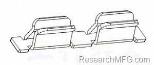
 For almost of the frequency radio apparatus, the Printed Circuit board must design the shielding frame/can to prevent the EMI (Electromagnetic Disturbance Interference) effect. The regular design will apply one shielding frame to mount on PCB by solder and another shielding can to cover on the frame to isolate the RF.
That means there will be two press tools cost before implement this solution. Beside, the shielding frame must be mounted on the PCB by SMT process. It requires lower flatness specification to keep the solder joint well. Most of the shielding frame asks its flatness meet 0.12mm maximum. Some of the shielding frame even asks the flatness must lower than 0.10mm maximum. Because of current stencil thickness is around 0.10~0.127mm only. It brings more difficult to form the shielding frame and raise its cost.

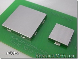
Actually, there is another choice of SHIELDING CAN CLIP that can be substitute of the shielding frame and provide lower cost and more efficiency. Here I make a comparison between the shielding frame and clip for the cost and maintenance as below table.
| Shielding Frame | Shielding Clip | |
| Photo | 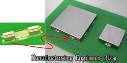 |
|
| Component cost |
Punch tooling one time charge about USD3,000~USD4,000 |
One clip: USD0.014 |
|
SMT constraint and cost |
|
|
|
SMT constraint and cost |
The cross rib on the frame will interfere with component while repair. Most of the time need to cut off the rib or damage the frame for repair. |
Easy to repair. |
|
Maintenance cost |
The test point can’t locate under the cross rib or frame edge. |
Easy to place the test point. |
|
Test |
Shielding-can is easily to place upon the frame without special training. |
Need special training for the operator to install shielding-can into it. |
|
Assembly |
Shielding-can is easily to place upon the frame without special training. | Need special training for the operator to install shielding-can into it. |
Even shielding clip has lots of advantages and cost profit, but there still has one big concern need to be care. There will be a small gap show between the shielding can and board. This will need RF engineer to double check its performance. 
I also list some of the data that shielding clip supplier provided as below.
- What is the clip force? How calculate the force to prevent it from drop while impact/drop test? According to the supplier answer that each clip will provide about 1Kgf force to hold the shielding can. So we will need to calculate the weight of shielding can and how many of gravity will be applied. Most of the shielding can need 4 clips will be ok that each side put one clip.
- What is the mounting force on the board? According to supplier answer that each clip can sustain 5kgf push force at least. It shall be OK for most of the consumer electronic products.
- How many of the distance shall put one clip? According to supplier answer to put one clip every 25mm will be OK.
- What is the stencil thickness? According to supplier answer that 0.1~0.12mm of stencil thickness is recommended. The thicker stencil thickness, the bigger gap show between shielding can and board.






Leave a Reply