Working for manufacturer engineering couple years. Sharing the manufacturing experience, skill, DFx, design, and information. Be care of this blog is personal share and content may not be 100% correctly.
A reader recently asked: “In surface mount assembly, PCBs often warp or bend after going through the reflow process, which can cause issues like open solder joints or tombstoning. How can we overcome this?”
To be honest, the reasons behind PCB warping or bending may vary, but they can generally be traced back to the stress applied to the PCB exceeding what the material can handle. When stress is uneven across the PCB or when different areas of the PCB resist stress unevenly, warping or bending occurs.
So, where does this stress come from? In the reflow process, the biggest source of stress is “temperature.” Temperature softens the PCB and can cause it to warp due to factors like gravity, the coefficient of thermal expansion (CTE), and the natural properties of materials that expand and contract with heat. These are the main causes of PCB warping and bending.
But why do some PCBs warp more than others?
Before diving deeper into this issue, Workingbear suggest you take a look at the article “The Real Causes of PCB Delamination and How to Prevent It,” as some of the concepts are related to what we’ll discuss below.
1. Uneven Copper Distribution on the PCB Worsens Warping and Bending — Pay Special Attention to Copper on the Edges
Most PCBs are designed with large copper areas for grounding purposes, and sometimes the Vcc layer also includes large copper areas. When these large copper areas aren’t evenly distributed across the PCB, they cause inconsistent heat absorption and dissipation, leading to different rates of expansion and contraction. This results in varying stress levels and potential deformation.
Additionally, when a PCB goes through the reflow oven and exceeds its Tg (glass transition temperature) limit, the PCB will start to soften. Combined with gravity or pressure, this can lead to deformation, and in some cases, permanent warping.
It’s worth noting that when designing a PCB, many people overlook whether there’s copper on the edges of the board. If there’s no copper on the edges, the board is more likely to warp under high temperatures. To combat this, most designers now reinforce the edges with copper arranged in a grid or dot pattern evenly to enhance the structural support.
2. Vias on the PCB Limit Expansion and Contraction
Most modern PCBs are multilayer boards, with layers connected by vias, similar to rivets. These vias can be through, blind, or buried holes. Wherever there’s a via, the board’s ability to expand and contract with temperature changes is restricted, which can also contribute to warping or bending.
3. The Weight of the PCB Itself Can Cause Warping
In most reflow ovens, the PCB is transported on chains that support the board by its edges. If the board has particularly heavy components or is larger in size, the weight can cause the center to sag, leading to warping.
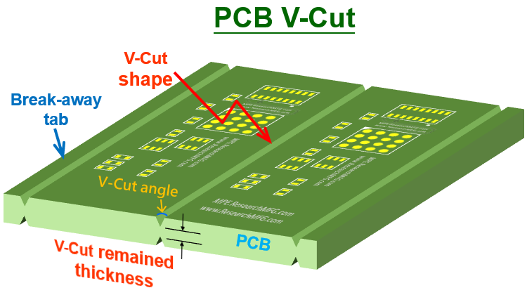
4. V-Cut Depth and Connection Strips Affect Panel Warping
V-Cuts are essentially the main cause of weakening the board’s structure. A V-Cut is a V-shaped groove cut into a large PCB panel, which makes that area more prone to deformation. (Related reading: PCB Edge Removal – V-Cut Machines).
How can we prevent warping and bending of PCBs during the reflow process?
1. Reduce the Stress Caused by Temperature
Since “temperature” is the main source of stress on the PCB, lowering the temperature in the reflow oven or slowing down the heating and cooling process can significantly reduce warping and bending. However, this might introduce other side effects, such as solder bridging.
2. Use High Tg Materials
Tg refers to the glass transition temperature, which is the temperature at which a material changes from a rigid glass-like state to a more flexible, rubbery state. The lower the Tg, the sooner and faster the PCB softens during reflow, increasing the likelihood of deformation. Using materials with a higher Tg can improve the board’s resistance to stress and deformation, though these materials tend to be more expensive.
3. Increase PCB Thickness
Many electronic products are designed to be thinner, so PCB thicknesses have been reduced to as little as 1.0mm, 0.8mm, or even 0.6mm. Keeping a PCB this thin from warping in the reflow oven can be difficult. If there are no strict thickness requirements, using a 1.6mm or more thick PCB can greatly reduce the risk of warping and bending.
4. Reduce PCB Size and Panelization
Since most reflow ovens use chains to transport the PCB, larger PCBs are more prone to sagging due to their weight during reflow. To mitigate this, align the long edge of the PCB with the reflow oven’s conveyor chain, reducing sagging caused by the PCB’s own weight. Reducing the number of panels for the same reason can also help. In other words, passing the narrow edge of the board perpendicular to the direction of the reflow conveyor minimizes sagging deformation.
If the other methods are hard to implement, the last option is to use a reflow carrier or pallet to reduce PCB warping. These carriers are typically made from heat-resistant materials like aluminum alloy or synthetic stone, which don’t deform easily. As the PCB goes through the high heat in the reflow oven and then cools down, the carrier helps keep it from bending. Once the PCB cools below its Tg (when it becomes rigid again), the carrier ensures the board stays in its original shape.
If a single-layer carrier doesn’t stop the board from warping, you can use a double-layer carrier with a lid to clamp the PCB between two layers (trays), which reduces warping even more. However, these carriers can be costly and require extra labor to place and remove them.


? Manufacturing Processes That May Generate Significant Stress")
? Increase the resistance of components to stress")
? The recommendation of BGA pad design from workingbear")
? Increase PCB stiffness to resist stress and avoid board bending")
? Stress is the Biggest Culprit in Causing BGA Solder Joint Cracks")

? Reduce the impact of PCB bending through the mechanism design change")


Leave a Reply