Workingbear personally doesn’t recommend using HASL (Hot Air Solder Leveling) surface-finished PCBs in today’s SMT reflow processes, especially for double-sided reflow or fine-pitch components located on 2nd side. The defect rate of soldering with HASL is quite high and hard to overcome.
Most people experienced with SMT processes, when facing issues with SMD components not soldering well, typically first suspect issues with solder paste printing (like improper stencil thickness, aperture, pressure adjustments), solder paste oxidation due to prolonged air exposure, moisture or oxidation on SMD component leads, or incorrect reflow oven temperature profiles.
Have you ever considered that a significant part of the soldering issues on HASL-finished PCBs might be due to insufficient tin thickness? For a while, most were familiar with soldering problems caused by insufficient gold or nickel layers on ENIG (Electroless Nickel Immersion Gold) finished PCBs. But can a thin tin/solder layer on HASL also cause soldering issues? Here is some information Workingbear has gathered for your reference (the images in the article are for reference only and are not case images).
Experienced friends are welcome to share your valuable insights.
Recently, Workingbear noticed a resurgence of HASL surface-finished boards. The reason seems to be the poor long-term reliability of OSP (Organic Solderability Preservative) finished boards. Initially, OSP can form a strong IMC (Intermetallic Compound) Cu6Sn5, but over time, it gradually forms the less desirable IMC Cu3Sn, leading to component detachment issues. This seems to be driving a subtle shift back towards HASL.
Moreover, after some process improvements, the surface flatness of HASL has also improved. Some PCB manufacturers are adding nickel (Ni) during the soldering process to slow down the formation rate of Cu3Sn, addressing the long-term reliability issues of HASL. So now, the only remaining issue is controlling the solder thickness.
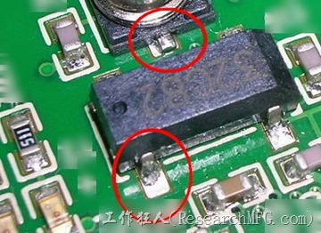
However, HASL surface-finished boards have a critical drawback: they tend to poor or cold solder joints (non-wetting) on the second side during double-sided reflow. The possible reasons are:
-
The first reflow process’s high temperature will remelt the solder on the PCB pads. This high temperature not only forms IMC (Intermetallic Compound) on the first side with printed solder paste but also on the second side without printed solder paste. If the solder layer on the second side is too thin, most of it may be used up during the first reflow. When the second side goes through reflow with printed solder paste, there is insufficient solder to form an effective bond with the paste, causing a significant drop in solder joint strength.
-
The high temperature of the first reflow will remelt the solder on the second side. As the temperature cools and the solder re-solidifies, it can cause uneven surfaces due to partial solder bump formation on the pads, leading to incomplete solder joints. This issue is particularly challenging for fine-pitch components and remains unresolved.
Collected online information about HASL defects:
| Article Title | Article Summary |
| Case Study on Soldering Defects with Lead-Free HASL (Simple Chinese) |
Metallographic analysis reveals that areas where solder fails to adhere on the pads have completely formed copper-tin alloys, which can no longer be soldered. Examining unsoldered PCBs from the same batch and performing cross-sectional analysis, it was found that the surface of the solder-coated pads already showed severe alloy formation (copper-tin IMC had formed). Workingbear speculates that this might be due to prolonged storage, causing copper-tin diffusion issues. The IMC thickness was measured at about 2µm. Considering that alloying increases thickness, it is inferred that the original solder coating thickness was below 2µm. Therefore, the root cause is determined to be the insufficient initial solder coating thickness (below 2µm) on the bare PCB, exposing the copper-tin alloy on the pad surface, leaving insufficient solder to bond with the solder paste, thus affecting the solderability of the pads. Metallographic analysis reveals that areas where solder fails to adhere on the pads have completely formed copper-tin alloys, which can no longer be soldered. Examining unsoldered PCBs from the same batch and performing cross-sectional analysis, it was found that the surface of the solder-coated pads already showed severe alloy formation (copper-tin IMC had formed). Workingbear speculates that this might be due to prolonged storage, causing copper-tin diffusion issues. The IMC thickness was measured at about 2µm. Considering that alloying increases thickness, it is inferred that the original solder coating thickness was below 2µm. Therefore, the root cause is determined to be the insufficient initial solder coating thickness (below 2µm) on the bare PCB, exposing the copper-tin alloy on the pad surface, leaving insufficient solder to bond with the solder paste, thus affecting the solderability of the pads. |
| How to Address Poor Soldering on Single-Sided Soldered Double-Sided Boards (Simple Chinese) Link has been lost |
This should be a summary article that compiles opinions from various sources, but most discussions ultimately attribute soldering issues to insufficient solder thickness. It is recommended that the solder thickness be at least 100u” (2.54µm) on large copper areas, at least 200u” (5.0µm) around QFP and peripheral components, and at least 450u” (11.4µm) on BGA pads. This helps mitigate the problem of solder rejection on the second side during reflow. However, the thicker the solder, the more prone fine-pitch components are to short-circuit issues. In PCB manufacturing, the smaller the pad, the thicker the solder layer tends to be. For fine-pitch components, controlling the amount of solder paste becomes more challenging, increasing the risk of shorts. The longer soldered boards are stored, the thicker the IMC (Cu6Sn5) layer grows, which negatively impacts subsequent reflow soldering. Generally, the flatter the solder on the board, the thinner the solder layer becomes. |
Possible Causes and Mechanisms for Poor Soldering and Wetting Issues on the Second Side of Double-Sided HASL Boards
This is a typical issue caused by insufficient solder/tin thickness on HASL boards. The general requirement for solder/tin thickness should be over 2.54µm on large copper pads, with a minimum of 2µm. It is recommended to have over 5µm the pad of QFP and peripheral components, and over 11.4µm on BGA ball pads.
During the first reflow on a double-sided HASL board, the solder on both sides has already been pre-applied. The high temperature causes the solder and the copper foil to react, forming a copper-tin intermetallic compound (IMC), specifically Cu6Sn5.
On the first side, the PCB will have solder paste, which provides enough solder to form IMC with the copper on the PCB surface and the metal surfaces of the electronic component leads, bonding the components to the PCB pads. However, on the second side, since there is no solder paste to provide additional solder, the IMC forms only with the existing solder coating and the base copper.
When the board goes through the second reflow, most of the original solder on the second side has already formed IMC with the copper during the first reflow, using up a significant amount of solder. If the remaining solder is insufficient to bond with the newly applied solder paste, it results in poor wetting on the second side. This explains why the solder paste tends to move to the component leads instead of wetting the pads, indicating that while the reflow temperature is adequate, the PCB surface is rejecting the solder.
Moreover, the already formed IMC has a melting point at least 10°C higher than that of SAC solder. To melt the IMC, you would need to increase the reflow oven temperature or extend the reflow zone time. However, this could potentially damage the electronic components, solder paste, and the PCB material. Therefore, the best solution is to require the PCB manufacturer to increase the solder thickness to ensure proper soldering.
Related Posts:


Leave a Reply