Working for manufacturer engineering couple years. Sharing the manufacturing experience, skill, DFx, design, and information. Be care of this blog is personal share and content may not be 100% correctly.
During new product development, electronics companies may encounter BGA solder ball cracking after a drop test in which the bare unit is dropped from a specified height. When this happens, the R&D team should take a systematic approach and perform a stress-strain analysis rather than immediately assuming that the BGA cracking is caused by the SMT process.
Based on Workingbear’s experience, BGA solder ball cracking is often difficult to resolve through SMT process controls or simply by increasing the amount of solder. In many cases, the root cause is related to the mechanical design of the product. Addressing the problem at the design stage can significantly reduce manufacturing costs and engineering effort later in the product life cycle.
In the case discussed below, a mechanical design change was able to eliminate the need for underfill, saving both material and labor costs. It also reduced the associated rework and engineering costs, improved product reliability, and lowered the risk of future quality issues in the field.
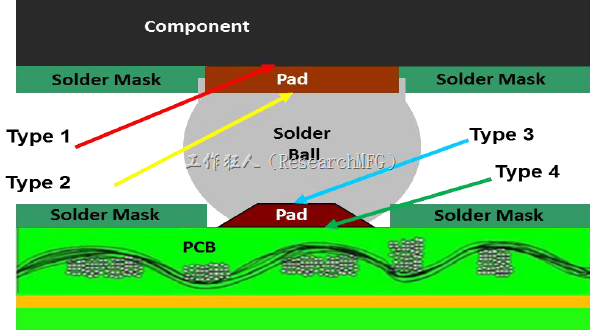
BGA solder ball cracking can involve many different factors, and soldering defects are only one of them. Unfortunately, when people see a cracked solder joint, their first reaction is often to assume that the soldering process is at fault. From a more scientific and objective perspective, however, if the solder joint shows a properly and uniformly formed IMC (Intermetallic Compound) layer, we can generally rule out major soldering-quality issues.
The next step is to consider the relationship between mechanical stress and solder joint strength. No matter how much we strengthen a solder joint, there is always a limit to how much stress it can withstand. Once the applied stress exceeds the strength of the solder joint, cracking is inevitable. Therefore, after confirming that the soldering quality is acceptable, we should investigate the source of the stress and look for ways to strengthen the mechanical design. In this case, the solder joint quality had already been verified, so the R&D team was asked to improve the mechanical design to reduce the impact of mechanical stress.
In fact, a large majority of BGA solder ball cracking problems are related to stress. The stress may come from PCB warpage during high-temperature reflow, mechanical stress during product assembly, or external impact caused by the customer dropping or otherwise mishandling the product. All of these can become sources of stress. If potential failure conditions are considered early in the product design stage, followed by stress-strain analysis and design changes to reduce the effects of mechanical stress or provide sufficient design margin, the manufacturing quality and reliability of BGA-based products can become much more stable. In some cases, unnecessary underfill processes can even be eliminated, resulting in additional cost savings.
I am not sure whether Workingbear’s repeated requests for stress measurements during previous new product development meetings finally made an impact, but this time the R&D team took a much more proactive approach. They performed a cause-and-effect analysis of the BGA solder ball cracking issue, identified the source of the mechanical stress, and made a design change to reduce it.
They first verified the improvement using a mechanical mockup, and the results were very encouraging. After the tooling was modified and the product entered production, the final QA verification also confirmed that no further BGA cracking occurred. I sincerely hope that this type of stress-strain verification can become a standard part of the R&D validation process for new products.
Using Strain Gauges to Compare PCB Strain Before and After the Mechanical Design Change
The following shows the approximate product design and the location of the BGA. To prevent screen glare and make the product easier for customers to use, the product was designed with a tilted display, similar to a cash register. However, this tilt angle caused the BGA to experience significant PCB deformation during top- and bottom-side drop tests, which eventually resulted in BGA solder ball cracking. No problems were found during side or corner drop tests. In previous cases, BGA failures had almost always occurred when the product landed on a corner.
Figcaption:BGA Solder Ball Cracking Improved Through a Mechanical Design Change
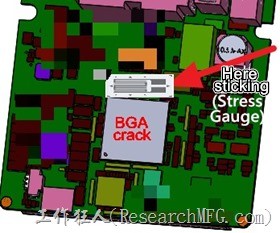
Once we identified excessive PCB deformation as a potential cause, we attached strain gauges to the PCB. We first measured the strain before the design improvement. Then, while keeping the PCB and other major components unchanged, we replaced the mechanical structure with the improved design and performed the same strain measurements again.
The improvement was to add a plastic structural rib near the BGA to support the PCB and reduce its deformation during a drop event. This is shown as [New Add Rib] in the figure above.
Figure: Pictues indicate the related location for BGA IC and new add rib.
Because most of the product design had already been completed when this issue was identified, the practical approach was to find available space where an additional support rib could be added. The goal was to provide a solid mechanical support point for the PCB during a drop, thereby reducing the amount of PCB deformation.
Figcaption:The BGA solder cracking improvement was to add a structural rib near the BGA to support the PCB and reduce its deformation during a drop event.
PCB Strain Before and After the Mechanical Design Improvement
The table below shows the measured microstrain (με) before and after the design improvement (addition of the rib). The values in the table are the actual measured values in units of ×10⁶. As expected, the strain during the top-side (tilted-side) drop test was reduced by 106 με. Because the top of the product has a curved, tilted profile, it is more susceptible to bending under external impact. In comparison, the bottom side has a flat surface, so the reduction in strain was smaller, at 42 με.
Unit: μɛ / Microstrain
Before Improvement
After Improvement
Reduction
Top-Side Drop
-186
-80
106
Bottom-Side Drop
203
161
42
Note: A commonly used industry guideline for acceptable microstrain is approximately ±450 to ±500 μɛ.
This result shows that adding a single structural rib can significantly reduce PCB deformation to a certain degree. The strain measurement in this case was taken in the Z direction at an X-axis location. It would have been even more useful to also measure the Z-direction strain along the Y-axis. When a PCB is dropped or subjected to an external force, the deformation is usually not a simple bend in a single direction. Bending can occur simultaneously in both the X and Y directions, and the board may even experience twisting. Measuring only one axis, such as the Z-direction strain along the X-axis, may miss significant deformation in another direction and therefore provide an incomplete assessment.
After implementing the mechanical design change, the improvement was re-verified through DQ drop testing. The results confirmed that the BGA solder ball cracking problem no longer occurred.








Leave a Reply