These soldering wrinkles appeared quite a while ago, but Workingbear recently came across a similar situation on an online forum. Thinking others might encounter the same issue, I decided to document it for both personal reference and to share with everyone.
Workingbear had previously noticed that some data transmission cable samples from a supplier had solder joints on the internal PCBA with wave-like wrinkles and what looked like cracks. At first, it was assumed that these were caused by cracked flux residue. However, even after cleaning the flux with alcohol, the same wave-like wrinkles were still visible, indicating that the issue was actually with the solder itself.
The potential reasons for these wave-like wrinkles or cracks on the solder joints are as follows:
-
The solder paste melting temperature was too low (the reflow peak temperature was insufficient), or the time spent in the reflow zone was too short. If the molten solder didn’t have enough time to fully melt, flow, and wet before the temperature started to cool down, wave-like wrinkles could form. It’s generally recommended that the peak temperature in the reflow zone be 245~255°C for SAC305, and 215~225°C for Pd63Sn37. The time above liquidus (TAL) in the reflow zone should be between 30 and 60 seconds, though some manufacturers may require more than 45 seconds.
-
Thermal shock or rapid cooling in the reflow oven. If the cooling rate is too fast and the liquid solder hasn’t fully fused and solidified before the temperature drops below its melting point, similar stress marks can appear.
-
Solder paste oxidation or premature flux evaporation. When solder paste oxidizes, a buildup of oxides can form on the surface of the molten solder, preventing the solder joint from achieving a smooth finish after cooling and solidifying. Additionally, oxidized solder paste can create internal voids in the joint, introducing stress that may cause the joint to crack or develop wrinkles.
Oxides usually float on the surface of the solder, forming a rigid shell. As the temperature drops and the solder begins to solidify, it contracts slightly inward. This inelastic oxide layer, attached to the outer surface of the solder, gets pulled inward during the cooling and contraction process, causing wrinkles to form in the oxide, which may also affect the shape of the solder it contacts.
If solder paste is left exposed to the air for too long without being used, the flux may evaporate and dry out prematurely. Without sufficient flux to remove oxides during reflow, wetting will be compromised, and wrinkles may form on the surface of the solder. -
High-humidity environments. High humidity accelerates solder paste oxidation, which can reduce the effectiveness of the flux and may lead to flux sticking to the solder joint and solder paste, causing internal voids in the solder joint.
-
In no-clean soldering processes, flux residue may form a transparent film on the solder joints after reflow. If the flux is exposed to thermal shock or solvents like alcohol, it can crack and cause a similar appearance. If it’s flux residue, there’s no quality issue, and you can clean it with a solvent to confirm.
In Workingbear’s case, microscopic inspection showed that the solder had formed a proper fillet, indicating the initial soldering was successful. The product was then subjected to high and low-temperature cycle testing, and no quality issues were found, so the batch was approved.

In this instance, we later requested the supplier to provide the reflow temperature profile. We discovered that the peak temperature during reflow was only around 236°C, and in one profile, the highest temperature was just 229°C. There was also significant variation in ramp-up times between different profiles, which indicated inconsistent solder melting times for various components. This inconsistency can easily cause the tombstone effect. For SAC305, the peak temperature seemed a bit low. Typically, if the peak temperature is low, the time above liquidus (TAL) should be extended to increase the time the solder paste stays in a liquid state. Therefore, Workingbear recommended that the supplier prioritize raising the peak temperature and lowering the ramp-up rate. Only then should they consider extending the TAL to further improve the process.

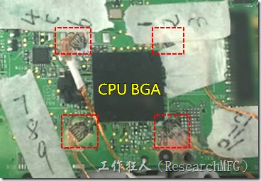
The other day, Workingbear encountered another similar case on an online forum (as shown in the image below), which was even more severe than the previous one.

The forum user later uploaded the reflow temperature profile for this PCBA, which seemed to use a leaded solder paste, as the reflow peak was only around 213.6 to 216.4°C—relatively low. The ramp-up rate was acceptable, and the TAL was about 68 to 73 seconds, which was also within an acceptable range. Generally, we recommend that the reflow zone temperature for Pd63Sn37 fall between 215~225°C.

In Workingbear’s case, microscopic inspection revealed that the solder had formed a proper arc, indicating that the initial soldering was effective. The product was then subjected to high and low-temperature cycle testing, and no quality issues were found afterward, so the batch was accepted.
So, both of these cases point out that the primary cause of wave-like wrinkles or cracks in solder joints after reflow is likely due to insufficient reflow temperature or time.
Of course, Workingbear’s perspective may not be entirely correct.
If you have different views, feel free to leave a comment and discuss!
Related Posts:


![[Case Study] Troubleshooting a Customer Complaint – Keypad Malfunction Caused by Oil & Powder Contamination on the PCB [Case Study] Troubleshooting a Customer Complaint – Keypad Malfunction Caused by Oil & Powder Contamination on the PCB](https://mpe.researchmfg.com/wp-content/uploads/2025/Oil_on_PCB_summary-mpe.jpg)


Leave a Reply