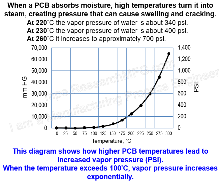
The Popcorn Effect in PCB and electronic components refers to the delamination (board cracking) or formation of bubbles when exposed to high temperatures during soldering. This phenomenon is similar to how popcorn pops—it happens because of trapped moisture inside. When heated, the internal moisture turns into steam, and as the temperature increases, the pressure from the steam rises. If this pressure exceeds the bonding strength of the component, PCB, or IC package, it causes a sudden expansion—just like a kernel turning into fluffy popcorn.
In PCBs, the Popcorn Effect results in delamination (layer separation) or blistering (bubble formation). In severe cases, visible white spots or bulging areas can appear on the board. In milder cases, the damage may not be visible externally, but internal defects remain, posing a hidden quality risk.
Three Key Conditions for the Popcorn Effect
For the Popcorn Effect to occur in electronic products, three conditions must be met:
-
Moisture Presence – There must be humidity (H₂O), which is naturally present in the environment.
-
High Temperature – The component or PCB must be rapidly exposed to high temperatures, typically above 100°C. The higher the temperature, the greater the steam expansion, making the effect more severe. Since H₂O boils at 100°C under normal atmospheric pressure, and PCB assembly (PCBA) soldering temperatures exceed 183°C (Sn63Pb37) or 217°C (SAC305)—sometimes even higher—this significantly increases the risk.
-
Trapped Moisture Space – There must be a semi-sealed cavity where moisture can slowly enter but cannot easily escape when heated. This applies mainly to IC packages and multi-layer PCBs, where layers are bonded together.
Causes of the Popcorn Effect in Electronic Components
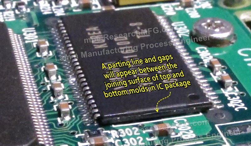
The Popcorn Effect in electronic components mainly occurs in packaged ICs. This happens because IC packages are formed by compressing Epoxy Molding Compounds (EMC) between upper and lower molds. Inside the package, there is also a lead frame with a bonded die (chip), and the leads extend out of the package body after molding.
Due to differences in material properties, there is a mismatch in the Coefficient of Thermal Expansion (CTE) between the EMC and the metal lead frame. When exposed to temperature changes, small gaps or micro-cracks can form at their interface.
Another potential issue is that air bubbles may get trapped inside the EMC during the molding process, especially near gold or copper bonding wires that connect the die to the lead frame. These conditions allow moisture to penetrate and accumulate inside the IC package. When the component undergoes high-temperature soldering during reflow, the trapped moisture rapidly turns into steam, expanding and causing the Popcorn Effect.
Popcorn Effect in PCB Assembly
In PCB assembly, the Popcorn Effect generally refers to board delamination or blistering due to high heat exposure. The term “Popcorn Effect” is more widely recognized in Western contexts. In professional IPC standards, the correct technical terms are:
✅ Blistering – Localized layer separation, which can cause visible swelling, whitening, or bulging on the PCB surface.
✅ Delamination – Separation between PCB layers. In severe cases, it can break through vias (conductive holes), leading to electrical failure.
Official IPC Definitions
🔹 Blistering: Localized swelling and separation between any layers of a laminate material, or between the base material and conductive foil or protective coating.
🔹 Delamination: Separation between layers within a base material, between the base material and a conductive foil, or any other planar separation in a printed board.
We previously mentioned that the Popcorn Effect doesn’t only happen to packaged ICs—it can also occur in PCBs. This is because a PCB is made by stacking and bonding multiple layers of copper traces and insulating materials together.
In a single-layer PCB, copper foil is essential for electrical conductivity. However, copper alone is too soft to provide the necessary structural rigidity, so other materials are added:
- Glass fiber – Used as a reinforcement to strengthen the board.
- Resin – Serves as the main material that holds everything together.
- Fillers – Added to improve mechanical and thermal properties.
📖 Recommended Reading: Introduction to the structure, characteristics and precautions of Printed Circuit Board materials
 If you take a close look at glass fiber, you’ll see that it consists of multiple thin glass filaments twisted into fiber bundles. These bundles are woven into glass fabric, where warp and weft fibers cross each other in a grid-like pattern.
The resin and fillers are used to fill the gaps between these fibers. However, if the glass fabric isn’t tightly woven, small voids and gaps can remain. These spaces can trap moisture, making the PCB more vulnerable to moisture absorption.
Once moisture gets inside the PCB, rapid heating during soldering can cause the trapped water to turn into steam, leading to delamination or board explosion.
📖 Recommended Reading: PCB Popcorn Effect: Why it Happens and How to Stop It
How to Prevent the Popcorn Effect in Electronic Components and PCBs During Soldering
Preventing the Popcorn Effect is actually quite simple. Since we know that three main factors contribute to this issue—moisture, trapped spaces, and high temperature—we just need to eliminate at least one of them. The real challenge is balancing cost and effort.
-
High Temperature: Unfortunately, finding a soldering material that works below 100˚C is nearly impossible. Extending the soldering time to allow moisture to escape is also inefficient. So, eliminating high temperature isn’t a practical solution.
-
Trapped Spaces in Materials: This would mean eliminating voids inside IC packages and PCBs, which can be done by modifying the materials. However, this approach is expensive.
-
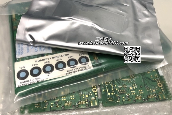
Moisture Control: The most practical and cost-effective method is controlling moisture exposure.
To address this, IPC has established standards for moisture-sensitive components and PCBs:
✅ J-STD-033 – Guidelines for handling, processing, and managing moisture-sensitive components (MSDs).
✅ IPC-1602 – Best practices for storing and handling moisture-sensitive PCBs.
These standards also provide baking procedures to remove moisture if components have been exposed to humidity for too long.
📌 Keywords: Moisture-sensitive components, Moisture Sensitivity Level (MSL), Popcorn Effect, Delamination
- The Hidden Dangers of Using Overdue PCBs: Can Baking Salvage Them?
- What Process Impact of Substituting SMDs with Paste-In-Hole components?
- What is IMC (Intermetallic Compound)? How does IMC relate to PCB solder joint strength? Are there IPC standards for IMC


Leave a Reply