The thriving development of the electronics industry owes much to the invention and improvement of Surface Mount Technology (SMT). Among the various SMT techniques, Reflow Soldering plays a pivotal role. In this discussion, we aim to shed light on some technical aspects and temperature settings related to reflow soldering.
The reflow profile for printed circuit board assembly generally consists of four major phases: Pre-heat, Soak, Reflow, and Cooling. This article represents a compilation of personal insights, and any corrections or suggestions are warmly welcomed.


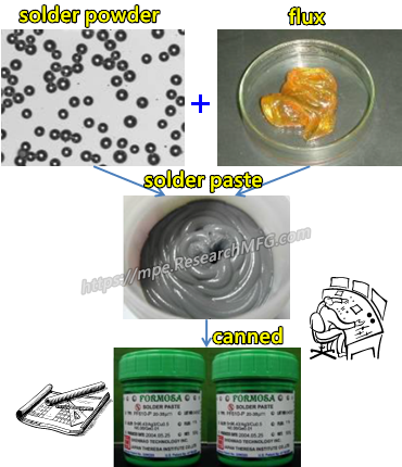
 Solder paste is a crucial material in the domain of modern electronic assembly technology. It is used for soldering electronic components onto printed circuit boards (PCBs), this enabling the creation of ever-evolving technological products.
