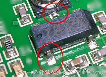
Workingbear personally doesn’t recommend using HASL (Hot Air Solder Leveling) surface-finished PCBs in today’s SMT reflow processes, especially for double-sided reflow or fine-pitch components located on 2nd side. The defect rate of soldering with HASL is quite high and hard to overcome.
Most people experienced with SMT processes, when facing issues with SMD components not soldering well, typically first suspect issues with solder paste printing (like improper stencil thickness, aperture, pressure adjustments), solder paste oxidation due to prolonged air exposure, moisture or oxidation on SMD component leads, or incorrect reflow oven temperature profiles.


