Working for manufacturer engineering couple years. Sharing the manufacturing experience, skill, DFx, design, and information. Be care of this blog is personal share and content may not be 100% correctly.
Hey folks, welcome back to the blog! Today, we’re diving deep into something absolutely critical for the reliability of almost every electronic gadget out there: BGA solder joints. You know, those tiny connections that hold complex chips onto our printed circuit boards (PCBs). Keeping them strong and free from defects like those pesky little bubbles inside the solder – we call them voids – often comes down to a surprisingly fundamental aspect: the design of the pads on the PCB.
Here at MPE ResearchMFG website, we’ve been tackling real-world problems in electronics assembly, doing our own experiments and getting hands-on with these challenges. We’ve relied on great source material, including articles and discussions, to explore the core questions: Which pad design, SMD (Solder Mask Defined) or NSMD (Non-Solder Mask Defined), holds up better against cracking under stress? And which design might help reduce soldering defects like voids?
Spoiler alert: There’s no simple answer. It’s definitely about trade-offs. What works best is highly dependent on the specific device, its needs, and what it has to withstand. Our goal is to help you get a better grasp of these choices and their implications.
First Off: What’s the Difference?
Let’s break down SMD versus NSMD. It’s all about the solder mask, that green coating on the board.
SMD (Solder Mask Defined): With SMD, the solder mask layer covers part of the copper pad. The opening in the mask dictates the size of the area where the solder ball connects. The mask effectively defines the solderable area.
NSMD (Non-Solder Mask Defined): Sometimes called “copper defined“, NSMD is the opposite. The copper pad is actually smaller than the opening in the solder mask. When you solder, the solder wets onto the top of the copper pad and also flows down and wets up the sides of the copper pad within that larger mask opening.
Think of it like this: with SMD, the green mask is defining the border. With NSMD, the copper itself defines the connection area, and the mask opening is larger.
Tackling the Stress Factor: Cracking
As devices become smaller and thinner, they are exposed to greater mechanical stress. We’ve observed BGA joint failures—even when underfill is applied, which is intended to reinforce the area between the BGA package and the PCB. This indicates that the stress levels can be substantial.
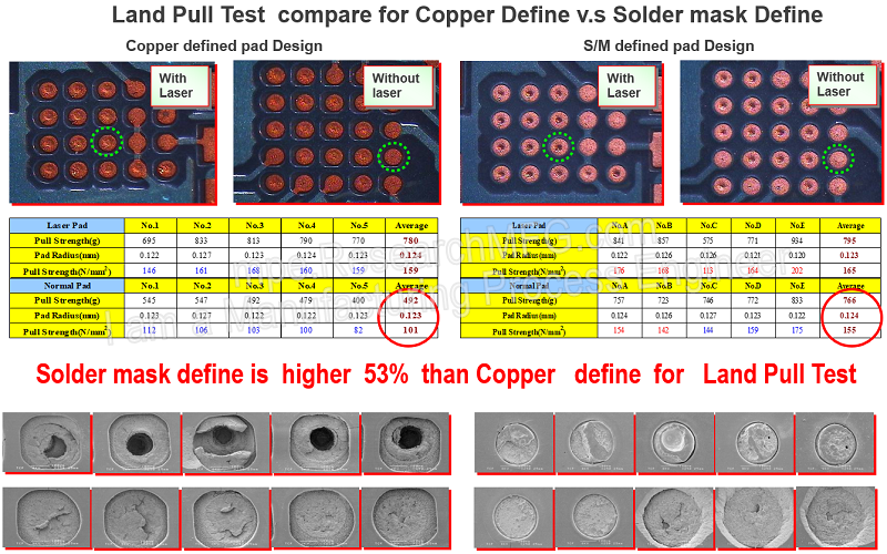
Initially, PCB manufacturers we talked to often suggested switching to an SMD design to fix cracking issues. The idea was that the solder mask overlapping the copper pad would anchor it more strongly to the underlying board material (FR4), making it harder for the entire pad to rip off under stress.
Did PCB manufacturers test this idea? Absolutely. They did some pull tests directly on the pads (without solder balls, just testing pad adhesion). In that specific test, SMD pads showed significantly higher pull strength – about 53% higher than NSMD.
Whoa, right? That sounds like a lot. But it’s crucial to remember that’s just the pad-to-board adhesion, not the strength of the entire solder joint with the ball attached. Useful information, but not the full story.
The Trade-offs: Strength vs. Solderability
So, SMD might seem stronger at the pad level, but what about the actual soldering process and the final joint?
NSMD often has advantages for soldering. Because the solder can wet onto the sides of the copper pad, not just the top, you generally get better solder wetting and easier bonding. Plus, NSMD pad size and position are defined by the copper etching process, which is usually more precise than placing the solder mask. Critically for designers, the smaller copper pad leaves more space between pads for routing tiny electrical traces, which is vital for fine pitch BGAs.
The flip side for NSMD is its potential weakness: that smaller copper area bonded to the board. It has less surface area adhering to the FR4, theoretically making it easier to tear off under stress. Also, the exact shape can sometimes be uneven where traces enter the pad. Products needing to pass drop tests often still need underfill with NSMD for extra robustness.
SMD’s big advantage for overall joint strength is that solder mask overlap acting as reinforcement. It holds the pad down more securely, improving adhesion to the FR4 and generally helping the joint survive drops and tumbles better. It’s like a picture frame holding the pad in place. This stronger foundation is key.
But SMD has downsides too, especially for soldering. The solder mask material can expand when heated during reflow, slightly changing the opening and potentially interfering with solder paste contact. Aligning the solder mask isn’t always as accurate as copper etching. And that larger copper area needed for the SMD overlap means less space between pads for routing traces, making board layout tougher.
It truly is a balancing act. As we found, there’s no single “best” way; it completely depends on the product’s specific needs, stress levels, board density, cost, and more.
What About Testing Actual Solder Joints?
Theory and pad-only tests are helpful, but we needed to test actual solder joints with the balls attached. We performed two main tests on soldered BGAs: a shear test (pushing the ball sideways) and a pull test (pulling the ball straight up).
We used common components: 0.4mm solder balls, standard 1.6mm thick FR4 TG-150 board with ENIG finish (Electroless Nickel Immersion Gold, good for solderability) , and SAC 305 lead-free solder. We should note our shear test speed (5,000 micrometers/sec) was faster than the standard specified range, so while useful for comparison between SMD and NSMD in our setup, the raw numbers might not be directly comparable to other standard tests.
Here are the results:
Pull Test: NSMD came out slightly ahead (884.63 gf average) compared to SMD (882.33 gf average). However, this was a very small difference, not statistically significant. Basically a tie in pull strength.
Shear Test: This is where it got interesting. NSMD performed significantly better in shear. NSMD averaged 694.75 gf, while SMD only averaged 639.21 gf. NSMD resisted that sideways push better.
The Impact of Via-in-Pad
We also looked at the effect of having plugged vias (filled holes) under the pads. Generally, having plugged vias tended to improve both pull and shear strength for both SMD and NSMD pads.
Here’s a weird twist we noted: NSMD with plugged vias gave the best results in the shear test, but SMD with plugged vias actually gave the best results in the pull test. That seemed counterintuitive and is something we feel needs more investigation – why the best performance switches depending on the stress direction. It highlights the complexity.
Switching Gears: Those Pesky Voids
Another big headache in soldering is voids – those tiny bubbles inside the solder.21 We’ve seen questions asking which is better for reducing voids: SMD or NSMD?
This is an area with conflicting advice. The common wisdom you often find online is that NSMD is better for voids. The theory is that the exposed copper sides give gas more pathways to escape during reflow. Seems logical, right? More escape routes.
However, someone in a forum mentioned an expert book claiming the opposite – that SMD is better for gas release, especially with lead-free solder. A direct contradiction!
Our practical experience here at mpe.ResearchMFG sides with the common consensus: we generally see slightly fewer voids when we use NSMD. We specifically saw a significant problem with a 0.4mm pitch BGA using SMD pads, resulting in large voids causing electrical shorts. Ouch! Shorts are bad news. Most people on the forum agreed NSMD usually meant fewer voids.
Other factors like large copper planes or silk screen near fine pitch BGAs can also affect things like board flatness or paste printing, potentially making voids worse. The general feeling is that for really small pitch parts, NSMD is often preferred, maybe even skipping silk screen nearby. For larger pitch BGAs, maybe SMD is okay, giving you the benefit of more consistent pad size and possibly better adhesion.
Our reasoning aligns with the common wisdom: NSMD exposes those vertical copper sides, providing more area for solder wetting, better flow, and critically, more ways for trapped gas to get out during reflow. We feel most research and experience point to NSMD for better joint quality and fewer voids, especially with BGAs.
Analyzing a Severe Void Problem
Regarding that specific case with the 0.4mm pitch BGA, SMD pads, and severe shorting voids: simply changing the pad definition might not be enough for such a severe problem. We suspected it was more likely related to the via-in-pad implementation, specifically how the via was filled. Perhaps there was a dimple left in the fill, or the resin used for filling outgassed during reflow, creating those big voids. This shows you have to look under the pad, not just at the edges.
The user provided a ton more detail, including X-rays showing shorts, board pictures, specs for a 0.4mm pitch WCSP (Wafer Level Chip Scale Package) with 0.28mm balls, a very thin 0.8mm stencil with tiny 0.21mm square openings (they’d downsized from 0.25mm due to previous shorts), a thin 0.7mm board, and a standard reflow profile. Overall voiding was under 8%, which isn’t terrible, but they had those specific large ones causing shorts.
We acknowledged that SMD pads can make paste printing trickier for fine pitch due to the solder mask thickness creating a small standoff between the stencil and board, affecting the paste deposit. However, SMD pad size is usually more consistent than NSMD where traces enter, which can help with stencil aperture design. So, consistency vs. potential standoff issues.
We remained skeptical about the claim that SMD is better for gas escape – it just doesn’t align with most evidence we’ve seen. For the void issue itself, we reiterated checking with the PCB fabricator about the via filling process, likely copper plating for that pitch.
An interesting point we raised was about the reflow atmosphere. We wondered if using nitrogen (N2) might counterintuitively be making things worse in some cases. How could nitrogen make voids worse? While it usually helps by preventing oxidation, the theory is that it might lower the solder’s surface tension and increase the internal pressure within forming voids, potentially making them larger or harder to collapse. It’s not definite, but something to consider. Another complex interaction!
Our main practical suggestion for the user with the shorting problem was to try experimentally reducing the solder paste volume even further, perhaps slightly smaller stencil apertures again. But do this carefully. We strongly recommended using SPI (Solder Paste Inspection) to accurately measure the deposited paste volume . You don’t want to reduce it too much and end up with insufficient solder or weak joints. Careful, measured experimentation is key. That case study really shows how many little things can affect the outcome – it’s rarely just one cause.
Wrapping Up
Picking between SMD and NSMD pads for BGAs is definitely not straightforward. It’s a mix of factors with no single best way for every design.
Here’s a quick recap of the main takeaways from our deep dive:
SMD pads generally offer better physical adhesion to the board and are often stronger against mechanical stress like drops. The mask helps hold them down.
NSMD pads generally offer better solderability. The solder wets more easily, and the exposed copper sides allow gas to escape more effectively, which can reduce voids. So, in general, it’s a trade-off: strength versus solderability and void performance.
Via-in-pad, especially when filled properly (copper electroplating microvia filling), seems to help improve strength and electrical performance for both SMD and NSMD. It’s generally a good practice if done right.
For preventing cracking, the number one thing is still good mechanical design of the whole device to minimize stress in the first place. Focusing only on the pad isn’t enough.
For soldering defects like large voids, you must look beyond the pad type. Via filling details, solder paste volume, the reflow profile, and even the atmosphere all play a part.
It really takes a holistic view of design and manufacturing. Understanding these trade-offs helps you make smarter decisions for your specific product and its reliability needs.
As electronic devices face ever tougher reliability demands – think handhelds, wearables, automotive, industrial environments – it’s fascinating to consider how PCB and packaging technologies will evolve. How can we get past some of the inherent limits of today’s BGA soldering and pad designs? It’s an ongoing challenge to keep pushing that balance between mechanical toughness, electrical performance, and manufacturability. Definitely something to ponder!
We encourage you to check out source materials and think about how this applies to your own work or the devices you use. Thanks for joining us for this deep dive!
《YouTube》Deep Dive: Comparing SMD and NSMD Pad Designs for BGA Solder Joint Reliability
《Podcast》EP024-Deep Dive: Comparing SMD and NSMD Pad Designs for BGA Solder Joint Reliability


 pads design. Refer to above picture show the solder mask open size is bigger than the copper pad size.")

. The copper pad size is bigger than the solder mask open area. That means the solder mask cover upon the copper pad and the soldering pad size will be defined by the solder mask open dimension.")


? Increase the contact area of solder to increase its strength")
 in SMT Reflow on Various Soldering Defects")
 in SMT Reflow Ovens: Optimizing Soldering Quality and Reducing Oxidation")


thank you for your work!