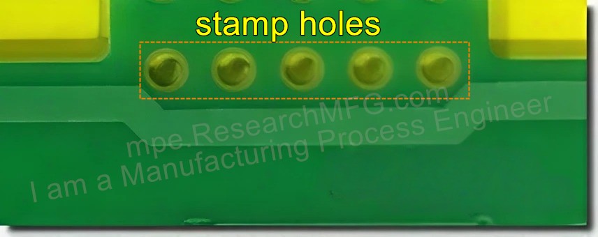
In most PCB (Printed Circuit Board) designs, panels are usually connected using V-cuts or tabs/ribs, and then separated with a V-cut scoring machine or a router de-panel machine. However, besides these two common connection methods, there’s another approach called the stamp hole design. Workingbear personally isn’t a big fan of this method, which is why it hasn’t been covered until now.
The name “stamp hole” comes from its resemblance to a sheet of postage stamps — small holes are drilled along the break line, allowing the boards to be snapped apart by hand or with pliers. This design makes manual de-paneling easy and doesn’t require special equipment, unlike the other two methods that need a scoring or routing machine.
However, the stamp hole design has several drawbacks:
-
Rough edges and burrs: After de-paneling, the board edges are often uneven and may leave burrs (flash), which can cause problems during assembly — especially for visible or precision areas such as displays. These rough edges can also cause mechanical interference or even functional issues.
-
Risk of damage: Since stamp-hole panels are usually broken manually, improper force can bend the PCB and lead to cracks in solder joints or components, reducing product reliability.
-
Unstable quality: Manual breaking tools and force vary from person to person, making quality control difficult.

Stamp holes are typically used for PCBs that can’t use V-cuts — for example, when the board is too thin. Thin boards with V-cuts can warp or lose strength after cutting. So in these cases, stamp holes are used instead.
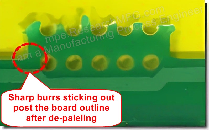
That said, designing stamp holes properly requires care. Poor designs often result in large burrs that stick out beyond the outline after separation. These burrs must be manually trimmed and sanded, which wastes both time and labor — and the dust can even contaminate nearby products.
The main difference between a good and a bad stamp-hole design lies in the placement of the connecting tabs.
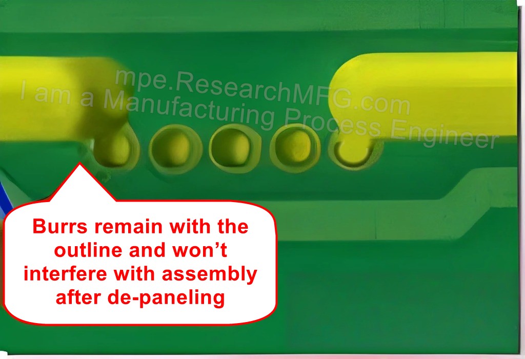
In a good design, the tab edge aligns with the middle of the outermost holes, which pre-weaken the break line. This makes it easier to snap the board cleanly and keeps burrs within the outline.
In a poor design, the tabs are placed incorrectly, causing the broken edges to protrude beyond the contour, requiring manual rework.
Poor Stamp Hole Design Example
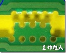
A bad design leaves sharp burrs sticking out past the board outline after de-paneling, requiring manual sanding. This wastes labor and increases cost, and the sanding dust can contaminate other boards. (In the example shown, only three holes are used, but the result is similar.)
Better Stamp Hole Design Example
A well-designed stamp hole still produces small burrs, but they remain flush with the outline and won’t interfere with assembly.
Recommended Methods for Separating Stamp-Hole Panels
Although some engineers choose stamp holes to save on de-paneling equipment, Workingbear strongly recommends not breaking boards by hand unless you’re absolutely sure the PCBA has no delicate components that could be damaged by bending stress.
Here are the proper methods for de-paneling stamp-hole boards:
-
Manual breaking: Using pliers to snap the board apart by hand. (Not recommended due to quality risks.)
-
Router de-paneling: Stamp-hole boards can also be cut with a routing machine. For details, see “PCB Edge Removal and De-paneling: Router Cutting Method.”
-
Laser cutting: Can also be used, but make sure no copper is placed near the cut path, since resin and copper require different laser power levels.
-
Punching fixtures: A custom punch tool can be designed to remove the tabs. Always fix the PCB securely before punching, and use a large-area clamping plate that won’t affect the circuit to prevent board warping.
Related Posts:





Leave a Reply