We all know that when producing PCBs and PCBAs, multiple individual PCBs are usually combined into one larger panel, a process called panelization, to improve production efficiency. Typically, these individual boards are arranged in a neat and consistent manner with the same orientation. However, when the PCB has an irregular shape or special requirements, a mirrored panel or flipped panel design might be used. While this design can improve efficiency in the SMT production line and reduce material costs, it may also come with certain design and production challenges. In this article, we will explore these issues and consider potential solutions.
For “flipped panel designs,” there’s a limitation—it’s not recommended to use this design on boards with heavy components. That’s because heavy components are typically placed on the second side to avoid the risk of falling off when they pass through the reflow oven a second time, as the solder paste melts again.
Even though it’s not recommended, there are ways to work around this issue. However, it might take some extra effort, and you’ll need to consider whether it’s worth the cost.
-
Method 1: You can dispense glue under the heavy components.
In the early days of Surface Mount Assembly lines, dispensing red glue was a standard process, and having a dedicated glue dispensing machine was essential. This allowed glued surface mount components to go through wave soldering. Nowadays, not every SMT line has this equipment because most components have shifted from PHDs (Plating Though-hole Devices) to SMDs. Alternatively, you could apply the glue manually, but I wouldn’t recommend it due to the difficulty in maintaining consistent quality with manual application.
-
Method 2: Use reflow carriers.

You can design reflow carriers to support heavy components, preventing them from falling off during the second reflow process. However, carriers are expensive, and you need enough of them to match or exceed the length of the reflow oven. You’ll need to calculate how many boards are in the oven at the same time, plus extra carriers for buffering and transporting. Basically, You’ll need at least 20-30 carriers to run the surface mount assembly. Carriers are usually made from metal or special high-temperature resistant plastics because they must withstand multiple passes through the high heat of the reflow oven. Also, keep in mind that using carriers adds extra labor costs, as someone will need to load and unload the boards onto the carriers.
-
Method 3: Hand solder the heavy components.
I wouldn’t recommend this method either, as it’s hard to control the quality with manual soldering, and some components are difficult to hand solder.
Additionally, when dealing with “mirrored or flipped panels,” another issue arises with boards layout that use components on one side that tend to absorb a lot of heat (such as large ATM card slots or metal shielded connector). These components require a longer heating time to reach the solder paste’s melting point, but care must be taken to avoid burning other more delicate components. For such boards, special attention needs to be given to adjusting the reflow temperature profile.
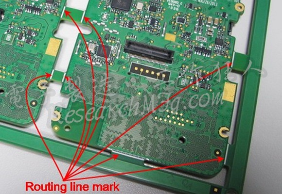
Regarding “irregular mirrored panels with the same side facing up and down,” they don’t significantly improve SMT line efficiency but do help save on board material. However, a key concern is how to cut the board edges and the tabs or ribs between individual PCBs. Typically, standard panel designs can use V-Cut for edge cutting, which helps reduce costs. However, with irregular mirrored panels, there are limitations, as V-Cut can only handle straight-line cuts. For curved edges or irregular outlines, a router machine is required. For more information, you can refer to the article on “PCB De-Paneling: V-cut scoring de-paneling and removing board edges.”
One common issue with panelization is the potential for X-out board defects, especially when more individual boards are combined into one panel. X-out board refers to a panel that contains one or more defective boards, and board manufacturers typically mark the bad board with an X using a marker, hence the name X-out board. Most SMT assembly factories prefer not to accept these boards, as they can reduce production efficiency. However, X-boards are an inevitable part of the manufacturing process. The more boards that are combined in a panel, the higher the likelihood of X-out boards, which increases the overall scrap rate and, in turn, the cost. PCB manufacturers generally prefer fewer boards per panel to minimize X-out board losses, but these costs are often passed on to customers if the problem persists.
Some professional OEM manufacturers will manually rework the panels using certain techniques, which can be quite impressive. For more details, you can refer to the article on Manual Panel Rework.
Related Posts:


Leave a Reply