If you’re an SMT engineer, you’ve probably used an X-Ray inspection machine to check the soldering quality of BGAs. But, after looking at the BGA solder balls repeatedly, they all seem to look the same. So, how can you tell if there’s a non-wetting issue?
Most people use X-Ray inspection machines to check for issues like solder shorts, insufficient solder, or bubbles/voids. However, using X-Ray to determine if BGA solder balls have non-wetting issues is a bit more challenging, especially with a 2D X-Ray machine. But if you’re careful, you can still find clues using 2D X-Ray images to determine if BGA solder balls have voids.
Generally, the images from X-Ray are simple 2D projection views (top-down views), which make it easy to check for solder shorts. However, using it to detect non-wetting can be difficult because every BGA solder ball appears almost round, making it hard to identify non-wetting or cold solder issues. While newer technologies like 3D CT X-Ray claim to detect non-wetting and HIP/HoP issues effectively, 3D X-Ray equipment is expensive, and even a single inspection can be costly. Moreover, the scanning speed is slow, and it’s uncertain if it can perform as well as advertised.
Here, Workingbear shares a tip on how to use traditional 2D X-Ray images to identify issues like non-wetting, cold solder, or HIP/HoP problems with BGA solder balls.
1. A Larger Diameter in BGA Solder Balls Could Indicate Solder Voids
Think about it: every solder ball in the same BGA package should be of the same size. If some solder balls in a single BGA have non-wetting, while most are soldered correctly, do you think there would be a difference in their shapes? The answer is yes. Ideally, when the same volume of solder ball is compressed, some of the solder in properly soldered balls will spread to the soldering pad on PCB, making the ball diameter smaller. However, solder balls with non-wetting won’t adhere to the pad and will instead expand in diameter after compression.
The image below shows that when a solder ball has a non-wetting, its diameter actually increases. It’s a good idea to compare the solder balls on a good board to see if they are all the same size since certain board designs can cause solder balls to be smaller, which will be explained further below.

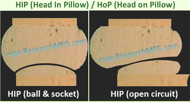
Workingbear also believes this increase in the solder ball size is closely related to HIP (Head In Pillow) or call HoP (Head On Pillow) and NWO (Non-Wet-Open) issues. However, it’s challenging to detect HIP and NWO with 2D X-Ray because the size variation of the BGA balls is minimal.
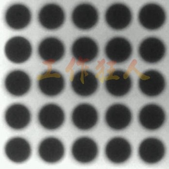
▼ The following image shows an example where the solder ball diameter is larger, indicating a non-wetting or cold solder joint.

▼ Can you spot which BGA solder ball has non-wetting in this X-Ray image? Hint: Use the method I mentioned above!

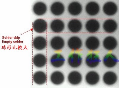
▼ Now, Workingbear has drawn a few lines. Can you see if one of the BGA solder balls is larger, suggesting a possible non-wetting? Check the previous image again to make sure you’re not mistaken. It’s just a slight difference!

Not satisfied yet? Here’s a practice exercise to let you experience “how to use 2D X-Ray to inspect BGA solder voids” firsthand.
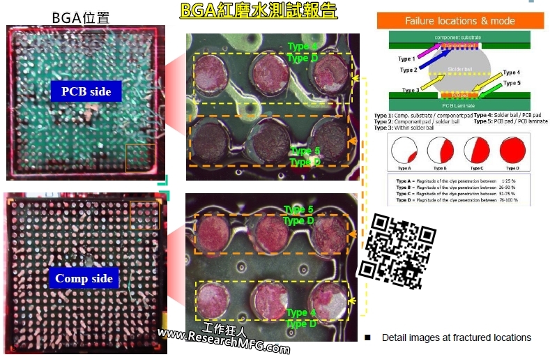
Note: This method cannot be used to detect cases where the BGA solder ball is broken due to stress impact, as these typically involve well-soldered boards that crack after experiencing stress, making it impossible to use solder ball size to identify the issue.
2. Vias Causing Insufficient Solder, Leading to Non-Wetting Solder
Another common cause of non-wetting for BGA soldering is insufficient solder, which typically happens when vias are present on the solder pads on PCB. During the reflow process, some of the liquid solder may flow into the vias due to capillary action, leading to insufficient solder on the pad. Even if the vias are designed next to the pad but aren’t isolated with a solder mask, this problem can still occur. In such cases, the solder ball’s diameter seen in the X-ray image will appear smaller. If too much solder is drawn into the vias, it can result in a void. Generally, it’s not recommended to place vias directly on the solder pads, and any vias near the pads should be covered with solder mask. In the future, we can discuss the pros and cons of via-in-pad designs and possible solutions.
Related Reading: Disadvantages of Vias-in-Pad and Handling Guidelines
▼Even with via-in-pad or via-on-pad designs that use plated filled vias, if the dimples are too deep after filling, similar issues can arise.

▼ This is an example of a poor design where the via is placed next to the solder pad. In this design, molten solder can easily flow into the via, causing insufficient solder and resulting in non-wetting issue.

3. Voids in Solder Balls Causing Non-Wetting Solder
Another cause of BGA non-wetting is the presence of bubbles/voids within the solder balls themselves. According to the updated IPC-7095B 7.5.1.7 standards, voids in BGA solder balls should not exceed 25% of the diameter or 6.25% of the area.
▼ When voids in the solder balls are large enough to impact solder quality, it can be clearly seen in cross-sectional images. In the example below, the void occupies about one-third of the solder ball.

▼ This X-ray image shows voids in the solder balls, with some voids being as large as 0.5d.

Related Posts:


Leave a Reply