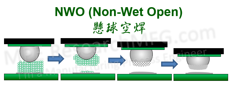
This is an X-ray inspection image of an MCU’s BGA soldering that failed after reflow. The owner mentioned that the BGA package was not functioning, but when pressing on the MCU, it would temporarily work again. Since Workingbear didn’t have the chance to see the faulty product in person, the assessment is based on this image alone. However, from the overall description given, this appears to be a typical case of BGA non-wetted. Can you spot the problem with the solder balls from the X-ray image above?
When examining 2D X-ray images of BGA solder balls, the main approach is to look at the size and shape of each ball. If you notice any balls that are significantly larger or smaller in diameter or that appear irregular in shape, these could indicate problematic solder joints. Workingbear strongly recommends having a control sample—a good BGA sample as a golden reference and a defective BGA sample for comparison. This helps ensure that you can accurately determine if there are issues with the BGA solder balls. For more background, you might refer to the article How to Use 2D X-Ray to Determine BGA Non-Wetting Solder to understand the two main causes of BGA solder voids.
However, Workingbear would like to clarify that a 2D X-ray cannot fully identify all solder issues in a BGA, such as the Head-in-Pillow (HIP) effect, which often shows minimal differences in ball size. For a more detailed analysis, it’s advisable to use 2.5D X-ray equipment that allows angled views, or 3D CT X-ray scanning, to get a clearer picture of the BGA solder conditions.
The X-ray image below comes from a sample assembled from the same batch of PCBs. To be honest, this board is also a failed board, but the soldering issues are relatively minor. Workingbear suggests using this X-ray as a reference for a good sample and comparing it with the first X-ray image at the beginning of this article. See if you can identify how many problematic solder balls there are.

In the design of this PCB, all vias-in-pad were processed with copper-filled vias, so there shouldn’t be issues of solder loss caused by vias wicking solder away. Also, voids in the solder balls seem to be under control, with no particularly large voids observed.
Therefore, the only likely issues could be the amount of solder paste applied, the accuracy of solder paste printing, the reflow temperature profile, solder mask misalignment, or whether board warpage has caused HIP (Head-in-Pillow) issues.
Related Reading: SMT Reflow Soldering Temperature Profiles Explanation and Precautions
Workingbear believes that the amount of solder paste and its printing precision might be critical factors causing the BGA failures on this board. Observing the failed BGA’s X-ray images, you’ll often see that solder balls with enlarged diameters are usually accompanied by smaller ones nearby. This suggests that during the reflow process, the larger solder balls have drawn solder away from the smaller ones, leading to the discrepancy in size. Comparing this to a reference good board can help confirm if the solder balls’ sizes are consistent.
Additionally, there appears to be deformation in the solder balls at the four corners of the BGA. This could be due to neighboring solder balls pulling on each other during the reflow process, solder mask misalignment causing pads to not form proper circles, or issues related to the HIP effect, which can lead to solder ball distortion.
Related Reading: Can Solder Mask Misalignment on PCBs Cause BGA Short Circuits?
And now, for the big reveal! (Workingbear realized after posting the image that there were still a few problematic solder balls that weren’t marked—oops! Did you spot them?)

▼ Top-left corner X-ray image.

▼ Top-right corner X-ray image.

▼ Bottom-left corner X-ray image.

▼ Bottom-right corner X-ray image.

Related Posts:
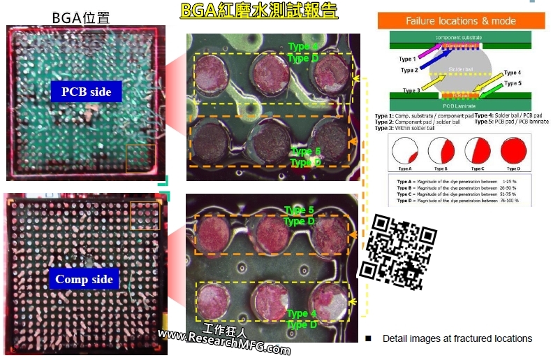
- Red Dye Penetration Test to check for BGA solder joint cracking
- Why BGA soldering ball always crack(1)? Stress > bonding-force
- When does SMT require Reflow Carriers and Full Process Carriers?
- SMT Reflow Soldering Temperature Profiles Explanation and Precautions
- How to Evaluate the Risk and Probability of Electronic Components Not Falling Off during SMT Second Reflow


Leave a Reply