 Solder paste is a crucial material in the domain of modern electronic assembly technology. It is used for soldering electronic components onto printed circuit boards (PCBs), this enabling the creation of ever-evolving technological products.
The invention of solder paste played a pivotal role in the miniaturization of electronic product assembly technology. It transformed bulky devices, such as early large sized mobile phones, into pocket-sized, feature-rich smartphones.
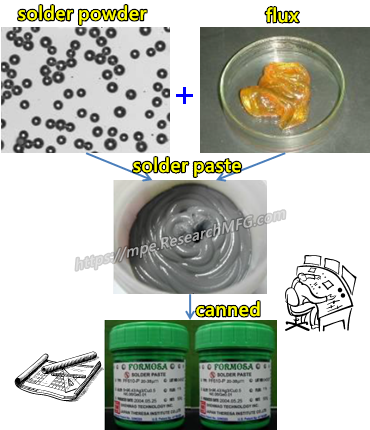
The term “paste” in solder paste is used because its pre-melted form is similar in consistency to the toothpaste we use daily. Before soldering, the paste-like solder can be applied to hold electronic components in place on the surface of the PCB. This ensures that these components remain in position, even under slight vibrations. Its primary function, however, is to solder electronic components onto the PCB, facilitating the connectivity of electronic signals.
read more…》

 Phenomenon in SMT Process")


