One of our company’s products once experienced an issue called an “internal micro-short” in the printed circuit board (PCB). After investigation, we discovered the root cause was something called CAF (Conductive Anodic Filament). But let’s be honest—if you translate that literally, hardly anyone would understand what it means! Simply put, CAF is a kind of hidden short circuit that forms inside a PCB layer or even under the solder mask (the green coating on the surface of circuit board).
This CAF problem has been stuck in Workingbear’s mind for a long time. Over time, and after taking some courses on PCB process and having deeper discussions with several PCB makers, Workingbear has finally put together some thoughts and findings on how CAF forms and how we might prevent it. Hopefully, this summary helps others understand the issue better.
Be noticed, Workingbear isn’t a CAF expert, so if you’ve got experience with it, feel free to share—everyone can learn more from each other!
How CAF Forms (The Mechanism)
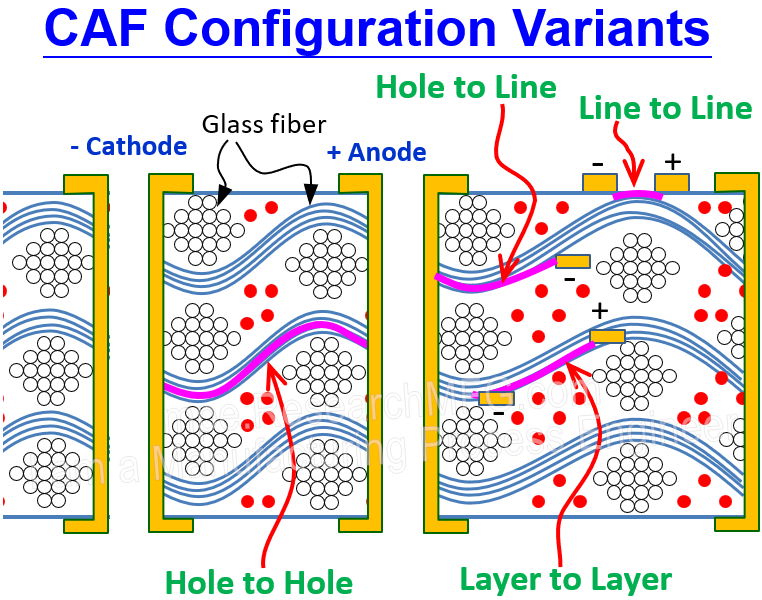
Take a look at the diagram at the top of this article to see how CAF forms. In short, CAF happens when a printed circuit board (PCB) is exposed to a direct current (DC) voltage and placed in a high-humidity environment. Moisture combines with contaminants to form an electrolyte. If there are tiny gaps between PCB layers, traces, vias (holes), or between a via and a trace, the copper at the higher potential (the anode) can oxidize into Cu⁺ or Cu²⁺ ions.
These copper ions then migrate along existing gaps—often between fiberglass strands—toward the lower potential (the cathode). As the ions move, electrons from the cathode travel toward the anode. When copper ions meet electrons, they reduce back into copper metal. But under continued bias voltage, this cycle repeats, and the copper slowly grows from the anode toward the cathode, forming a conductive path. This is sometimes called “copper migration.”
A lot of people get frustrated when they first encounter CAF because the symptoms come and go. Once the CAF path is complete, it may conduct electricity—but heat from the current can burn the path and temporarily break the short. So when you measure it with a multimeter, sometimes you’ll see a short, and sometimes you won’t. Even when you try to recreate the failure, it may only appear randomly. As long as the conditions for CAF exist, this on-off behavior can keep repeating in the same location.
What Causes CAF (Conductive Anodic Filament)?
Based on experience, CAF only happens when all four of the following conditions are met. If even one is missing, CAF won’t occur. So really, CAF is never just a “random” issue—it’s a chain of failures:
-
Moisture – From the environment or solvents. Even leftover flux or salty sea air can become electrolytes.
-
Ionic material (like exposed copper) – Since PCBs are made with copper foil, this can’t be avoided. Copper and silver are especially prone to CAF.
-
Electrical bias – A voltage difference is necessary. Even different metals in contact (dissimilar metals) can create a potential difference (Galvanic effect).
-
A migration pathway – This is the only factor we can realistically improve. It usually means the physical distance between nodes and the quality of insulation.
Electrochemical Migration (ECM)
CAF is really a form of electrochemical migration (ECM), where metal ions move through a non-metal medium under the influence of an electric field and form a conductive bridge between the anode and cathode.
Anode Reactions:
-
Cu → Cu²⁺ + 2e⁻ (copper dissolves)
-
H₂O → H⁺ + OH⁻
Cathode Reactions:
-
2H⁺ + 2e⁻ → H₂ (hydrogen gas)
-
Cu²⁺ + 2OH⁻ → Cu(OH)₂
-
Cu(OH)₂ → CuO + H₂O
-
CuO + H₂O → Cu(OH)₂ → Cu²⁺ + 2OH⁻
-
Cu²⁺ + 2e⁻ → Cu (copper re-deposits)
Two-Stage Theory of CAF
Most experts believe CAF formation happens in two stages:
-
Stage One – Path Creation: Under high humidity, the silane coupling agents used between the resin and the reinforcing material undergoes chemical hydrolysis (break down), which leads to the formation of a leakage path along the reinforcing material within the epoxy-resin/fiber structure. This stage is reversible.
- Stage Two – Electrochemical Growth: Under bias voltage, copper ions migrate and deposit, forming a conductive bridge. This stage is irreversible, and once it happens, it causes a short circuit between traces or layers.
How Can We Prevent or Fix CAF Issues?
To solve or prevent CAF (Conductive Anodic Filament), we can go after any of the four key factors mentioned earlier. If we eliminate even just one of them, CAF won’t happen.
1. Use PCB Materials with Better Anti-CAF Performance
The materials used for PCBs play a major role in preventing CAF. But as always, better materials cost more. Most Anti-CAF base materials require special ordering. Here are some tips for choosing good Anti-CAF materials:
-
Reduce ionic contamination in the material.
-
Make sure the fiberglass is fully and evenly soaked in resin.
During PCB base manufacturing, fiberglass bundles are woven into fabric and soaked in resin. If the soaking isn’t done well, gaps may form inside the bundles—CAF loves those gaps.
Introduction to the structure, characteristics and precautions of Printed Circuit Board materials -
Use resins that absorb less moisture.
-
Consider flat or spread glass fabric (open yarn designs).
2. PCB Layout Design: Bias and Hole Spacing
The layout—like where you place vias, traces, and how you stack the layers—strongly affects the chances of CAF. As products get smaller and denser, PCB spacing shrinks, but PCB process capability has limits.
When bias voltage is present and spacing between lines gets smaller, CAF risk goes up. Higher voltage or shorter distances = more risk.
Here’s what many PCB manufacturers recommend for CAF prevention:
-
Minimum via-to-via spacing: 0.4 mm
-
Minimum via-to-trace spacing (Drill to Metal): 12 mil (0.3 mm)
-
Recommended drill size: 0.3 mm
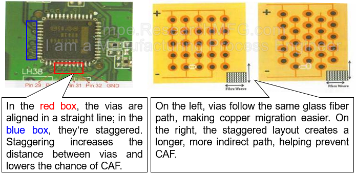
Also, CAF usually follows along a single glass fiber bundle. If you arrange your vias or pads at 45° angles, it may help reduce the risk.

3. Controlling Wicking During PCB Fabrication
When drilling vias (mechanically or with lasers), heat can go beyond the resin’s Tg (glass transition temperature), causing melted resin—called smear—to stick to the hole walls or inner copper edges. This leads to poor plating.
Before plating, we remove this smear in a process called desmear. The first step uses a chemical called a sweller, which soaks the board for 1–10 minutes, swelling the smear for easier removal.
However, overdoing it can cause copper wicking—where copper flows into the glass fibers, making later CAF problems more likely. Some manufacturers increase the sweller tank temperature to speed things up, but that can worsen the wicking issue.
According to IPC-A-600, here’s the max allowed copper wicking:
-
Class 1: ≤ 125 µm (4.291 mil)
-
Class 2: ≤ 100 µm (3.937 mil)
-
Class 3: ≤ 80 µm (3.15 mil)

That said, today’s requirements are stricter. If via spacing is only 0.4 mm, and copper wicking eats up 0.1 mm on each side, only 0.2 mm is left—that’s tight. Most PCB makers can now keep wicking below 50 µm (2 mil).
Some system companies have even reduced via-to-via spacing to 100 µm (4 mil), which makes CAF prevention even tougher.
Also, if the drill speed is too fast or the drill bit is worn out, it can tear the fiberglass, leaving gaps that allow CAF paths to form.
4. Preventing Moisture in PCB Assembly
During PCB assembly—like solder paste printing, part placement, and reflow—some residues may be left behind. These might include solder paste, adhesives, dust, or condensation. All of these can become electrolytes and trigger electrochemical migration (ECM).
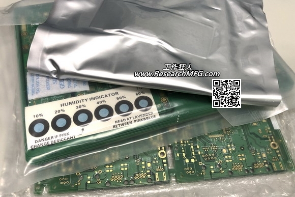
One solution is to seal any potential CAF-prone gaps using conformal coatings or sealants to block moisture.
Related Posts:


Leave a Reply