

A user asked: “During the SMT process, PCBs often warp or bow after going through reflow high temperature. In severe cases, this can lead to defects like insufficient solder joints or tombstoning. How can we prevent and solve this issue?”
To be honest, the reasons behind PCB warping and bowing may vary, but in the end, it all comes down to one key factor—when the stress applied to the PCB exceeds the material’s ability to withstand it. If the PCB experiences uneven stress or different areas of the board have varying resistance to stress, warping and bowing will occur.
What Causes Stress on a PCB?
The biggest source of stress during reflow is temperature. Heat softens the PCB and can cause it to twist or bend. When you add gravity, differences in the coefficient of thermal expansion (CTE), and the natural expansion and contraction of materials due to heating and cooling, you get the primary causes of PCB warping and bowing.
Why Do Some PCBs Warp More Than Others?
Before diving deeper into the causes, you may want to check out [The Real Causes of PCB Delamination and How to Prevent It] for additional insights related to this topic.
1. Uneven Copper Distribution Worsens PCB Warping and Bowing (Pay Attention to Copper Layout Near Board Edges)
Most PCBs include large copper areas for grounding, and some Vcc layers also feature extensive copper coverage. If these large copper areas are not evenly distributed, they can lead to uneven heat absorption and dissipation. Since the PCB expands and contracts with temperature changes, if different areas expand at different rates, internal stress builds up, causing deformation.
If the board’s temperature reaches its Tg (glass transition temperature) limit, it will soften, and the deformation may become permanent.
A key design tip:
Many engineers overlook copper distribution near PCB edges. If the edges lack copper, the board is more prone to deformation at high temperatures. However, simply adding copper to the edges isn’t enough—it should be evenly distributed, often in a grid or dot pattern, to enhance structural support.
2. Vias Restrict PCB Expansion and Contraction
Modern PCBs are mostly multilayer boards, where layers are connected by vias, including through-holes, blind vias, and buried vias. These via connections restrict the PCB’s natural expansion and contraction during heating and cooling, which can contribute to warping and bowing.
3. PCB Weight Can Cause Sagging Deformation
Most reflow ovens use conveyor chains to transport PCBs, supporting them by their edges. If a PCB has heavy components or is too large, the weight of the components and the board itself can cause sagging in the middle, leading to board warping.
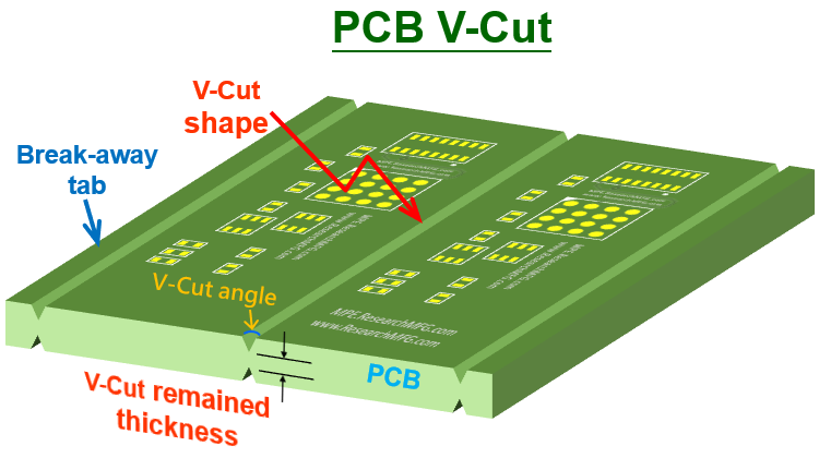
4. V-Cut Depth and Connecting Tabs Affect Panel Warping
V-Cut is often the main culprit behind PCB structural weakening. Since a V-Cut is essentially a groove cut into the PCB panel, areas with V-Cuts are more prone to deformation.
(Related reading: PCB De-Paneling: V-cut scoring de-paneling and removing board edges)
How to Prevent PCB Warping and Bowing During Reflow
So how can we prevent PCBs from warping and bowing when they go through the reflow oven? Below list the ideas and solutions.
1. Reduce Temperature Stress on the PCB
Since temperature is the main cause of PCB stress, lowering the reflow oven temperature or slowing down the heating and cooling rate (temperature ramp) can greatly reduce warping and bowing. However, this might cause other issues, such as solder bridging or non-wetting solder joints.
2. Use High-Tg PCB Materials
Tg (Glass Transition Temperature) is the point where a material transitions from a rigid, glassy state to a soft, rubber-like state. The lower the Tg, the faster the PCB softens in the reflow oven, leading to more severe deformation. Using high-Tg materials helps resist stress and deformation, but they are more expensive.
👉 Read more: What is Glass Transition Temperature (Tg)?
3. Increase PCB Thickness
To make electronics thinner and lighter, PCB thickness has been reduced from the standard 1.6mm to 1.0mm, 0.8mm, or even 0.6mm. Thinner boards are much harder to keep flat in the reflow oven. If thickness is not a strict requirement, using 1.6mm-thick boards can significantly reduce warping risks.
4. Reduce PCB Size and Panelization Quantity
Since most reflow ovens use chains to transport PCBs, larger boards can sag due to their own weight, causing bending and deformation.
- To minimize sagging, place the long edge of the PCB along the conveyor chains during reflow.
- Reducing the number of PCBs in a panel can also help.
👉 The Benefits of Using “Mirrored Panelization” for PCBs
👉 PCB Board Edge Removal and Panelization: Pros and Cons of Router Panel Cutting

5. Use Reflow Carriers or Fixtures
If the above methods aren’t practical, using reflow carriers (fixtures) is another solution.
- Reflow carriers are typically made of aluminum alloy or synthetic stone, materials that resist high temperatures and maintain their shape.
- They help keep the PCB flat as it expands and contracts in the reflow oven.
- For extra support, a top cover can be added to hold the PCB firmly in place, reducing deformation even further.
- The downside? Reflow carriers are expensive and require extra labor to load and unload.
👉 Why do thinner PCBs will need carrier for reflow process?
👉 When does SMT require Reflow Carriers and Full Process Carriers?
👉 The Benefits of Using SMT Synthetic Stone or Aluminum Alloy for Reflow Carriers


6. Use a Mesh Belt Reflow Oven
For single-layer PCBs, a mesh belt reflow oven can support the entire PCB during reflow, preventing sagging due to component weight. This method is also useful for the first pass of double-sided PCBs—just ensure the bottom side doesn’t get damaged by contact with the mesh belt. Some manufacturers place a non-stick paper under the PCB to prevent damage.
7. Use a Router Instead of V-Cut for Depaneling
Since V-Cut weakens the PCB’s structural strength, it’s best to avoid it or at least reduce its depth. Instead of V-Cut, router depaneling is a better option.
👉Reader more: What Is Router Cutting for PCB Depaneling? Advantages and Disadvantages Explained

Related Posts:
- How to Resolve HIP or HoP Soldering Issues in BGA Solder Balls
- Why BGA soldering ball always crack(8)? Increase PCB stiffness to resist stress and avoid board bending
- Why BGA soldering ball always crack(12)? Manufacturing Processes That May Generate Significant Stress

? Manufacturing Processes That May Generate Significant Stress")
? Increase the resistance of components to stress")
? Increase PCB stiffness to resist stress and avoid board bending")


Leave a Reply