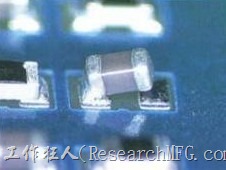
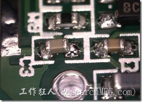
 Recently, some people have asked about issues with solder empty in small chip SMD components like resistors and capacitors. Even after thoroughly checking the reflow oven profile settings and confirming everything is correct, solder empty still frequently occur with these components, often in fixed positions. Observations of the solder also don’t show any signs of non-wetting or de-wetting, leaving many puzzled.
In reality, the cause of solder empty in these components isn’t that hard to understand! It’s essentially the same reason tombstoning occurs. To put it simply, it all comes down to this: “The solder paste on the two terminal ends of the component melts at different times, resulting in uneven forces and causing one side to lift.”
If you closely examine the copper traces on the problematic PCB, you’ll often find that one side of the component is connected to a large copper area, while the other side isn’t. When the PCB enters the reflow oven and begins heating up, the copper on the PCB’s surface heats up faster since it’s closer to the heat source, reaching the reflow oven’s ambient temperature sooner. In contrast, large copper areas on the PCB’s inner layers heat up more slowly, taking longer to reach the same temperature.
When the solder paste on one side of the component melts before the other, the earlier-melting side acts as a pivot point and lifts the component’s other side, causing it to detach from the solder joint and creating a solder empty. The greater the time difference in solder paste melting between the two ends, the larger the angle and height of the lifted component, which can ultimately result in the component standing completely upright—forming the tombstone effect.
For those interested in a deeper understanding of the mechanics behind tombstoning, you can approach the problem from a physics perspective. When the pulling force on one side exceeds the other (liquid solder has a high cohesive force, which pulls on the component’s solder joint), and you factor in the component’s weight and center of gravity, the component will pivot around one end and lift the other side.
The images below show examples of solder empty on a product, shared with permission from the owner for discussion and reference. Feel free to share your thoughts or insights!


Solutions to Prevent Tombstoning and Solder Voids in Small Components
-
Design Improvements
✔ Add thermal relief design to pads that connected to large copper areas to slow down heat dissipation.
✔ Reduce the distance between the two solder pads (also call as “air gap”) as much as possible without causing solder short. A smaller distance gives the slower-melting solder paste more area to hold onto the component, making it harder to lift and reducing the chance of tombstoning.
✔ If one pad uses SMD (Solder Mask Defined) design and the other uses NSMD, the pad sizes can become mismatched. This might not be a big problem for components larger than 0402, but for 0201 or smaller, the solder paste volume may not match the pad size. Uneven pulling forces during melting can lead to tombstoning. -
Process Adjustments
✔ Increase the temperature of the soak zone in the reflow oven to bring it closer to the melting temperature of the solder. You can also reduce the ramp rate when transitioning from the soak zone to the reflow zone. The goal is to ensure that all copper areas and components on the PCB heat up evenly, so the solder on both ends melts at the same time.
(Note: Arbitrarily adjusting the reflow oven’s temperature profile may cause other issues. Refer to the article “SMT Reflow Soldering Temperature Profiles Explanation and Precautions” for proper guidance.) -
Turn Off Nitrogen (N₂)
If nitrogen gas is used in the reflow oven, try turning it off and evaluate the results. While nitrogen prevents oxidation and improves solderability, it can also speed up wetting after the solder melts, leading to certain joints wetting earlier than others. This worsens the time difference in solder melting between the two ends, causing a larger force imbalance and ultimately resulting in tombstoning.
(Recommended Reading: Benefits and Drawbacks of Using Nitrogen (N2) in SMT Reflow Ovens: Optimizing Soldering Quality and Reducing Oxidation) -
Poor Tantalum Capacitor Material
Some tantalum electrolytic capacitors may have manufacturing defects, leaving behind incomplete decomposition of Mn(NO₃)₂. During lead-free reflow soldering at high temperatures (210–250°C), this substance decomposes and releases NO₂ gas, which can blow away or tilt the component itself and nearby parts.
Mn(NO₃)₂ → MnO₂ + 2NO₂↑
If this issue occurs, the best solution is to replace the tantalum capacitor. Alternatively, the capacitor can be preheated in a high-temperature reflow cycle beforehand.
(For further reference, a PDF research article on the theory of gas release in tantalum capacitors is available.)
Other Considerations:
The causes mentioned above are just some of the possible reasons for solder empty and tombstoning. Other potential factors include:
-
Oxidation on one side of the component or pad.
-
Misalignment when placing the component.
-
Feeder instability leading to inaccurate component pick-and-place.
-
Solder paste misprinting. Misprinting issues can be aggravated by large panelization; the larger the panel, the higher the chances of misalignment.
-
Significant differences in solder paste volume between the two ends of the pad. Smaller components like 01005 are especially difficult to control due to the reduced aperture size in the stencil. Consider using solder paste with a smaller particle size (higher number) or higher-quality stencils with smoother vertical profiles to improve solder paste deposition.
-
Placement machine precision issues.
Lastly, under the same conditions, capacitors (C) are more prone to tombstoning and open circuits than resistors (R). This is because resistor terminals only have solderable surfaces on three sides, while capacitors have five solderable surfaces, including the left and right sides. Additionally, capacitors are generally thicker, resulting in a higher center of gravity, which makes them easier to lift with the same amount of force.
Here are some videos that Workingbear found online explaining the causes of tombstoning and solder voids. Feel free to watch them for a better understanding of how these issues occur.
This video shows tombstoning caused by one end of the capacitor melting the solder first, while the other end melts later.
This video demonstrates a tombstoning scenario where one end of the capacitor melts the solder first, and the other end melts afterward, leading to the issue.
This video illustrates a case where the capacitor placement is misaligned. Although both ends of the component melt the solder at the same time, the misalignment results in one end having significantly more solder contact area than the other. The uneven solder pulling forces exceed the weight and balance of the component’s center of gravity, causing it to tombstone.
In all three videos, the solder paste that melted first acts as the pivot point for the tombstoning effect. However, the next video is worth closer analysis as the tombstoning occurs with the other end acting as the pivot point. In this case, you can observe that the solder on the initially melted side fails to wet immediately with the component terminal, allowing the solder on the other side, which melted later, to dominate and cause the tombstone effect.
Related Posts:


Leave a Reply