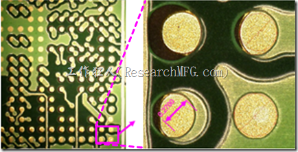
Over the past few days, Workingbear came across an issue I hadn’t really considered before. Here’s the story: an EMS (electronics manufacturing service) factory reported that during SMT production, they were seeing solder shorts under BGA components. After digging into it, the root cause turned out to be excessive solder paste. And why was there too much solder paste? The PCB’s solder mask (the green layer) and silkscreen (the white ink) were printed too thick.
When you think about it, this makes sense. If the solder mask or silkscreen is unevenly thick, it can affect the solder paste thickness during solder paste printing through stencil aperture. A thicker layer lifts the stencil slightly, increasing the gap between the stencil and the PCB. With all other printing conditions unchanged, that small gap leads to extra solder paste being deposited.
Has anyone else seen this kind of issue before?
Here are the basic specs for the BGA in question:

- Ball pitch: 0.65mm
- Ball diameter: 0.36~0.46mm
- Ball height: 0.23~0.33mm
According to the EMS factory’s report, this PCB was supplied by two different vendors. Measurements showed that the solder mask and silkscreen thickness between the two suppliers differed by 27.1 μm.

Under the same stencil printing conditions, boards from these two vendors produced nearly a 16.6% difference in solder paste volume. Based on this, the EMS factory concluded that the BGA shorting problem was caused by the PCB vendor.

To be honest, Workingbear has some doubts about this conclusion.
- First, if solder paste volume has such a big impact on BGA shorts, why didn’t the SPI (solder paste inspection) machine catch this problem right after printing? Why did it only show up later during X-ray inspection after reflow? Isn’t that too late?
- Second, does this mean the process margin for solder paste volume is really that small? Can PCB vendors truly control solder mask and silkscreen thickness so precisely? If not, won’t the same problem keep happening in future production?
Actually, this 16.6% solder paste difference can be adjusted by tweaking the squeegee speed or pressure during printing. Since the issue comes from the stencil-to-board gap, printing parameters can compensate for it.
The real key is whether SPI is set up properly to monitor not just the solder paste area, but also the paste height and total paste volume per pad. Only then can you maintain consistent solder paste quality.
📖 Related reading: How to print solder paste on PC Board and screen printing notices?
Finally, PCB vendors should also have clear specifications for solder mask and silkscreen thickness. These should be checked as part of incoming inspection, to prevent long-term yield problems in mass production.
Related Posts:


![[Case Study] Troubleshooting a Customer Complaint – Keypad Malfunction Caused by Oil & Powder Contamination on the PCB [Case Study] Troubleshooting a Customer Complaint – Keypad Malfunction Caused by Oil & Powder Contamination on the PCB](https://mpe.researchmfg.com/wp-content/uploads/2025/Oil_on_PCB_summary-mpe.jpg)


Leave a Reply