Working for manufacturer engineering couple years. Sharing the manufacturing experience, skill, DFx, design, and information. Be care of this blog is personal share and content may not be 100% correctly.
In discussions about printed circuit boards (PCBs), you’ll often hear the term Solder Mask (S/M). But what exactly is a solder mask, and what role does it play in a PCB? Some also refer to it as solder resist.
What Is a Solder Mask?
As the name suggests, a solder mask is used to prevent solder from accidentally adhering to areas that shouldn’t be soldered during assembly. The color you see on a PCB is actually the printed solder mask layer, not the natural color of the PCB material.
Over 99% of PCBs in the market use a green solder mask, but don’t be mistaken—solder masks come in other colors too, such as red, black, blue, and white. Different colors may be chosen for specific purposes. For example, during the NPI (New Product Introduction) phase, R&D teams sometimes use red solder masks to distinguish prototype boards (EVT/DVT stages) from mass production boards. Similarly, black solder masks are often used for exposed PCBs to match the color of an enclosure.
Why Is Green the Standard Color for Solder Mask?
The dominance of the green solder mask comes from historical advantages. In the early days of PCB manufacturing, green solder mask materials were the easiest to obtain and the most cost-effective. Over time, green became the industry standard, and many manufacturing processes and inspection systems were optimized for it.
For example:
AOI (Automated Optical Inspection) uses red light to detect PCB features, which works well with green solder masks but can cause visibility issues with red solder masks.
Laser barcode scanning is commonly used on PCBs for tracking and identification. Green is preferred because it provides good contrast, whereas other colors might reduce readability.
Although these challenges can be overcome with customized technologies, alternative solder mask colors often come at a higher cost due to lower compatibility with standard processes.
The Purpose and Function of Solder Mask
A solder mask is applied to the top and bottom layers of a PCB, covering the copper traces to protect them from oxidation and unintended soldering, which could impact the functionality of the assembled PCB (PCBA).
Because of this, solder masks are typically made of resin and are applied using silkscreen printing, covering areas where soldering is not required. This provides benefits such as:
Moisture resistance
Electrical insulation
Solder prevention
High-temperature resistance
Aesthetic appeal
For high-precision applications, some manufacturers now use inkjet printing instead of traditional silkscreen printing for even finer control over solder mask application.
The Meaning of “Mask” in Solder Mask
In Solder Mask, the word “Mask” actually refers to a photomask used in the manufacturing process.
When PCB manufacturers apply solder mask, they first coat the entire PCB with solder mask ink. The board then goes through a pre-baking process to dry the surface of the solder mask (but not fully cure it). Next, a film (photomask) is used for contact exposure, transferring the image from the film onto the solder mask layer—much like how a photocopier works.
Important Note: The image on the film is a negative. This means that black areas on the film indicate sections that should be removed, while the transparent areas allow the solder mask to remain. This is why the term “mask” is used—it acts as a stencil to control which areas of the solder mask are kept.
Next, UV (ultraviolet) light is used to fully cure the exposed solder mask, making it permanently bond to the PCB. This is why the earlier pre-baking step only partially dries the solder mask. Finally, the board is placed in a chemical bath to wash away the solder mask in areas covered by the photomask, exposing the copper surface underneath.
This exposed copper is where soldering will occur, which is why you might have heard engineers use the term “solder mask window”—it refers to areas where the solder mask is intentionally removed to expose the copper pads for soldering.
Important Note: The copper pads exposed after the solder mask process are not yet finished. A surface finish (such as ENIG, immersion silver, HASL, or immersion tin) must be applied to prevent oxidation before the board undergoes SMT (Surface Mount Technology) or wave soldering in an EMS factory.
Can Solder Mask Affect SMT Soldering Quality?
The solder mask process might seem straightforward, and its main role is simply insulation and solder prevention, but poor solder mask application can lead to serious quality issues.
Common solder mask defects include:
Contamination
Pinholes
Incomplete coverage
Exposed copper
Uneven thickness
Poor via plugging
Beyond these defects, misalignment and thickness variations in the solder mask can significantly impact SMT soldering quality—especially for high-density PCBs used in smartphones and other miniaturized devices.
Can Solder Mask Misalignment Cause BGA Soldering Short?
Yes! Since solder mask is applied using a photomask, alignment between the solder mask layer and PCB features is critical. If the alignment is off, the solder mask ink might partially cover solder pads, reducing their effective size and potentially causing BGA (Ball Grid Array) defects.
Additionally, the thickness of the solder mask affects solder paste deposition. A thicker solder mask increases the height difference between the mask and the solder pads, leading to more solder paste being deposited when using a stencil printer.
For large solder pads, this isn’t a problem.
For small solder pads, excess solder paste can lead to solder bridging and soldering short.
This is why solder mask thickness and alignment must be tightly controlled to ensure reliable soldering, especially for BGA components.
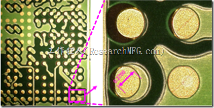
Solder Mask Printing Process Capabilities
Most PCB manufacturers use a squeegee and stencil to print solder mask onto the board. However, if you take a close look at a PCB, you’ll notice that its surface isn’t perfectly flat. The board has copper traces and large copper areas that protrude slightly, which can affect the thickness of the solder mask during printing. Additionally, due to the way the squeegee applies the ink, the solder mask can sometimes be thinner at trace corners (A).
Larger PCB manufacturers typically measure and control the solder mask thickness at four key areas (as shown in the diagram). However, the specific tolerances vary between manufacturers, and there doesn’t seem to be an industry-wide standard. In general, manufacturers avoid printing the solder mask too thin to prevent exposed copper and ensure proper coverage of vias. Factors such as stencil thickness, squeegee type and pressure, and the number of passes (usually one pass in each direction) all influence the final thickness.
Estimated Tolerance Ranges for Solder Mask Thickness
(These values are based on Workingbear’s research from multiple PCB manufacturers. They are for reference only, as different manufacturers may have their own specifications.)
A: Line Corner (Trace Corner): 0.2–0.8 mil
B: Line Area (Trace Area): 0.4–0.8 mil
C: Copper Surface Area (Solder Mask on Copper Plane): 0.6–1.4 mil
D: Base Material Area (Solder Mask on Substrate): 0.8–1.8 mil
Precision of Solder Mask Printing
Aside from thickness, the accuracy of solder mask alignment is even more critical. Due to cost constraints, most PCB manufacturers still use low-cost image transfer techniques for solder mask application, meaning the registration accuracy is not very precise. This can be a problem for high-precision applications, but as the saying goes, “You get what you pay for.” Higher-end imaging technologies are available, but they come at a premium.
Below are general capabilities of most PCB manufacturers regarding solder mask printing precision and minimum feature sizes:
E: Minimum Solder Mask Dam/Bridge (Smallest Solder Mask Feature): 4 mil (some manufacturers can achieve 3 mil).
The solder dam is the solder mask applied between adjacent pads to prevent solder bridging. The term “dam” doesn’t mean the mask physically blocks molten solder but rather that the solder mask has lower surface energy than the molten solder, causing the solder to retract back onto the pad. This is due to solder’s high surface tension, which naturally pulls it back to areas that accept soldering, much like how water flows downward.
F: Tolerance of Solder Mask Exposure Registration (Alignment Accuracy): ±2 mil (some manufacturers claim ±1 mil).
If the PCB uses a Non-Solder Mask Defined (NSMD) pad design, the registration accuracy affects the gap between the solder mask opening and the pad.
G: Should be the same as E.
Final Thoughts
Workingbear isn’t a PCB manufacturer or an industry insider—just someone who frequently works with PCB factories during product design and production. After repeatedly nagging and probing different PCB suppliers, I gathered and compiled this information for my own reference.
If you have specific questions about PCB manufacturing, it’s best to consult with the experts at your PCB factory. They’ll know more than Workingbear! Also, I can’t guarantee that all the information here is 100% accurate, so as always—think before you use it!

? What Is Its Purpose on a PCB? Why Is It Usually Green?")
,也會有大面積的銅面,這些浮出電路板表面的銅箔實際上或多或少會影響綠漆印刷的厚度,而且因為刮刀的影響,在線路轉角(Trace corner, B)的位置有時候會特別薄。")


Leave a Reply